Insulated gate field effect transistor and manufacturing method thereof

A field effect transistor, insulated gate type technology, which is applied to the insulated gate type field effect transistor and its manufacturing field to realize the reduction of feedback capacitance, can solve the problems of limited high-frequency switching characteristics, etc., to reduce on-resistance and improve high-frequency characteristics, the effect of reducing the number of masks

Inactive Publication Date: 2007-04-04
SANYO ELECTRIC CO LTD
View PDF1 Cites 15 Cited by
  • Summary
  • Abstract
  • Description
  • Claims
  • Application Information

AI Technical Summary

Problems solved by technology

[0015] However, since the integral value of the region x is determined by the drain-source voltage VDS applied to the MOSFET in the on state as shown in Fig. 17(B), there is a limit to improving the high-frequency switching characteristics.

Method used


Image

  • Insulated gate field effect transistor and manufacturing method thereof
  • Insulated gate field effect transistor and manufacturing method thereof
  • Insulated gate field effect transistor and manufacturing method thereof

Examples


Embodiment Construction

[0069] Referring to FIGS. 1 to 15 , an embodiment of the present invention will be described by taking an n-channel MOSFET as an example.

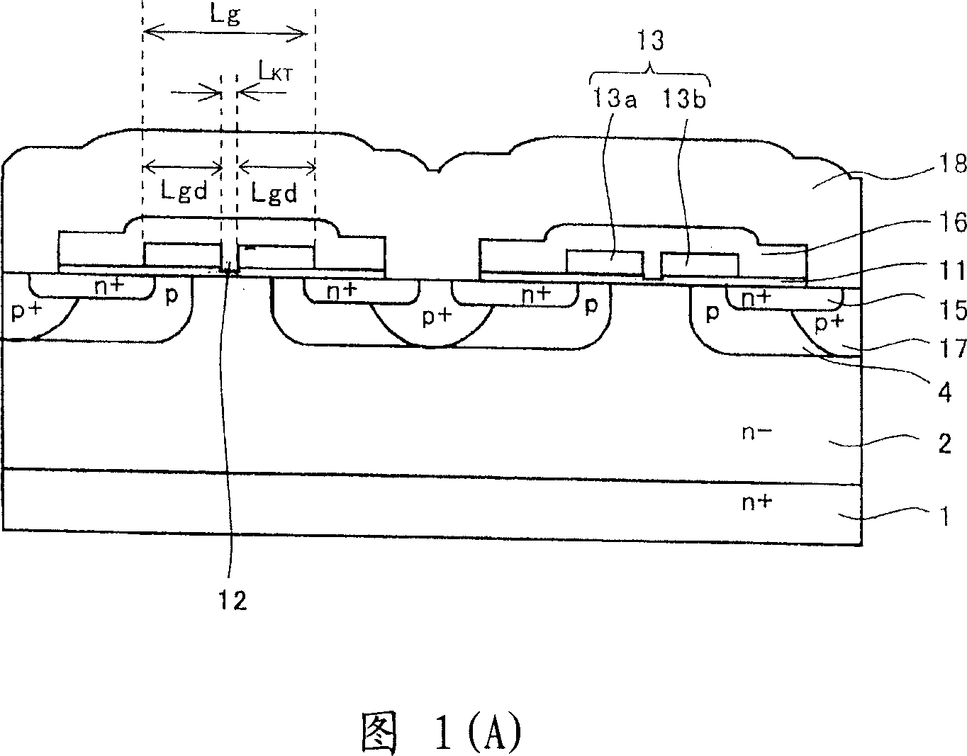
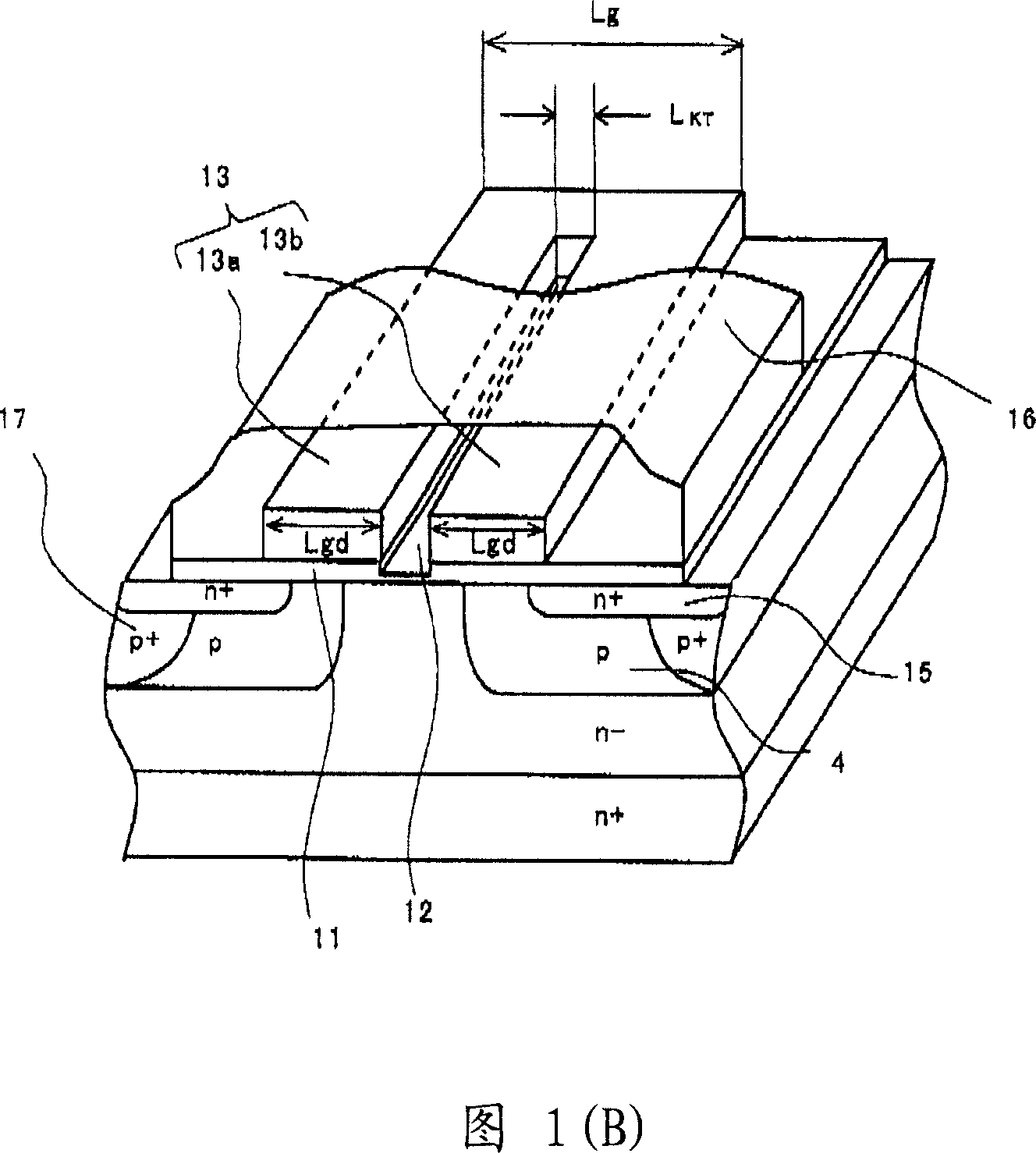
[0070] FIG. 1 is a diagram showing the structure of a MOSFET of the present embodiment of the first embodiment. FIG. 1(A) is a sectional view, and FIG. 1(B) is a perspective view.

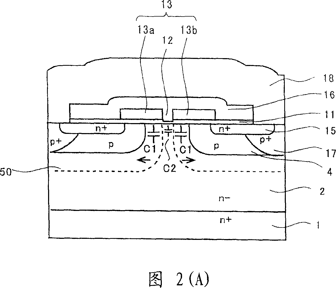
[0071] The MOSFET has a semiconductor substrate 1 , a semiconductor layer 2 , a channel region 4 , a gate electrode 13 , a separation hole 12 , a gate insulating film 11 , an interlayer insulating film 16 , a source region 15 , and a body region 17 .

[0072] For example, an n-type epitaxial layer 2 is stacked on an n+ type silicon semiconductor substrate 1 to provide a drain region. A p-type channel region 4 is provided on the surface of the n-type epitaxial layer 2 . A plurality of channel regions 4 are provided on the surface of the epitaxial layer 2 by ion implantation and diffusion. In addition, there are cases where a low-resistance layer is formed on ...


PUM


Abstract

A separation hole is provided in the center of the gate electrode. Accordingly, it is possible to suppress a drastic increase in feedback capacitance Crss in the case where drain-source voltage VDS is decreased and the width of the depletion layer is narrowed. Thus, high-frequency switching characteristics are improved. Moreover, n type impurities are implanted from the separation hole to form an n type impurity region between channel regions. Since a resistance in a portion below the gate electrode can be reduced, an on-resistance can be reduced. The n type impurity region can be formed in a self-aligning manner.

Description

technical field [0001] The invention relates to an insulated gate field effect transistor and a manufacturing method thereof, in particular to an insulated gate field effect transistor capable of reducing feedback capacitance and a manufacturing method thereof. Background technique [0002] Referring to FIG. 16, a conventional insulated gate field effect transistor will be described taking an n-channel MOSFET as an example. [0003] As shown in FIG. 16, an n-type semiconductor layer is stacked on an n+-type silicon semiconductor substrate 21, and a drain region 22 is provided. A plurality of p-type channel regions 24 are provided on the surface of the drain region 22 . A gate electrode 33 is provided on the surface of the n − -type semiconductor layer 22 between adjacent channel regions 24 via a gate insulating film 31 . The periphery of the gate collector 33 is covered with an interlayer insulating film 36 . In addition, an n+ type source region 35 is provided on the sur...

Claims


Application Information

Patent Timeline
Patent Type & Authority Applications(China)
IPC IPC(8): H01L29/78H01L29/423H01L29/10H01L21/336H01L21/28
CPCH01L29/41766H01L29/0878H01L29/66712H01L29/66727H01L29/7802H01L29/42372H01L29/4238
Inventor 栉山和成冈田哲也及川慎石田裕康佐山康之
Owner SANYO ELECTRIC CO LTD
Why Eureka
Try Eureka