

Embedding method for printed circuit board and printed circuit board
A printed circuit board, the first technology, applied in the direction of printed circuit, printed circuit manufacturing, printed circuit assembly of electrical components, etc., can solve the problems of unfavorable promotion and application, high production cost, expensive price, etc., to improve flexibility, The effect of saving process and cost
- Summary
- Abstract
- Description
- Claims
- Application Information
AI Technical Summary
Problems solved by technology
Method used
Image

Examples
Embodiment Construction
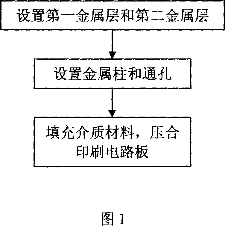
[0023] The present invention is further elaborated below in conjunction with accompanying drawing and embodiment:
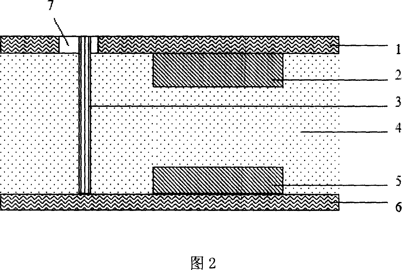
[0024] Refer to FIG. 1 for the flow chart of the method for embedding capacitance on a PCB in the present invention. The present invention can be embedded in any position on the PCB, and the specific process is as follows:
[0025] The first step: by means of electroplating or etching, a first metal layer is provided on the first surface of the power supply layer to increase the thickness of the metal, and a second metal layer is provided on a corresponding area on the first surface of the ground layer parallel to the power supply layer to Increase the metal thickness in this area; thereby reducing the distance between the power supply layer and the ground layer in this area, which is conducive to the formation of plate capacitance; wherein, the corresponding area is located on the first surface of the ground layer with an area opposite to the first metal layer, ...
PUM
 Abstract
Description
Claims
Application Information