Printed circuit board

A technology for printed circuit boards and plug-in holes, which is applied in the fields of printed circuit, printed circuit, and printed circuit manufacturing. It can solve the problems of poor soldering of plug-in components and large heat dissipation area, so as to reduce the area, slow down the heat dissipation speed, and avoid welding. bad effect

Inactive Publication Date: 2007-05-02
HONG FU JIN PRECISION IND (SHENZHEN) CO LTD +1
View PDF0 Cites 2 Cited by
  • Summary
  • Abstract
  • Description
  • Claims
  • Application Information

AI Technical Summary

Problems solved by technology

Due to the strong thermal conductivity of the metal layer 41 and the large heat dissipation area, after the printed circuit board passes through reflow soldering, the plug-in assembly will be poorly welded due to excessive heat dissipation.
Therefore, in the design of the metal layer of the printed circuit board, it is necessary to improve it to avoid poor soldering of the plug-in components due to excessive heat dissipation

Method used


Image

  • Printed circuit board
  • Printed circuit board

Examples


Embodiment Construction

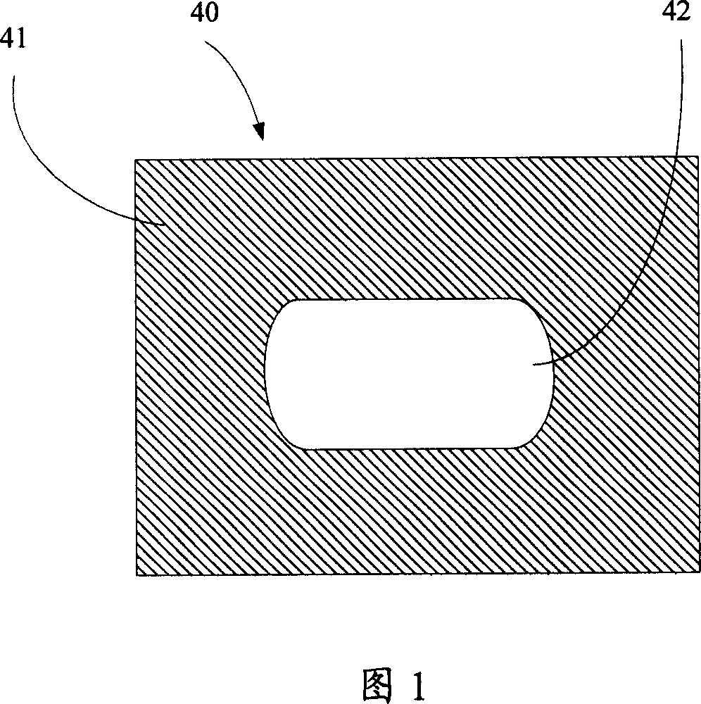
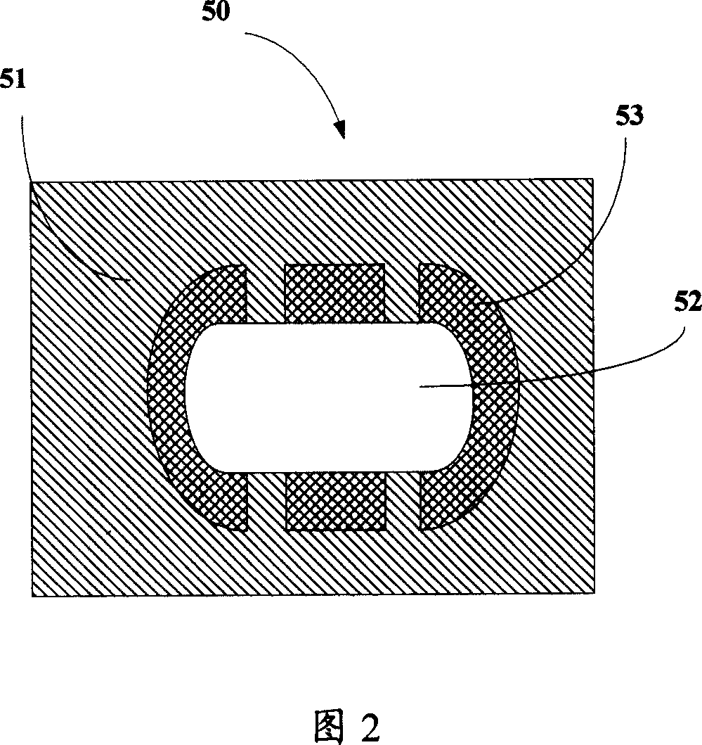
[0011] Please refer to FIG. 2 , which is a schematic plan view of the metal layer of a preferred embodiment of the printed circuit board of the present invention.

[0012] A printed circuit board 50 includes a metal layer 51 , an insertion hole 52 , and four insulating regions 53 , and the insulation regions 53 are spaced apart from each other and surround the insertion hole 52 . The metal layer 51 is a layer of copper foil, and the copper foil around the insertion hole 52 is separated by the insulating area 53 to form a strip, and the metal layer 51 is inserted into the insert through the strip. The plug-in assembly in hole 52 conducts. The width of the insulating region 53 is 14 mils. The strips were 15 mils wide.

[0013] Compared with the existing printed circuit board, the present invention reduces the heat dissipation area of ​​the copper foil around the plug-in hole of the metal layer of the printed circuit board, slows down the heat dissipation speed of the printed c...


PUM


Abstract

A PCB includes a metal layer and a plug hole characterizing that the metal layer of said PCB also includes several insulation regions surrounding the plug hole in intervals and the metal around the plug hole is isolated by the insulation regions, and said metal layer is conducted with the plug components in the hole by the metal isolated by the insulation layer, which reduces area of copper foil around the plug hole and slows down the radiation speed of said PCB after reflow soldering.

Description

【Technical field】 [0001] The present invention relates to a printed circuit board (Printed Circuit Board, hereinafter referred to as PCB). 【Background technique】 [0002] In multilayer printed circuit boards, the power layer and the ground layer usually use a whole piece of copper foil as the line, which is generally called "metal layer", and is connected to the signal layer of the printed circuit board through the plug-in component and its leads. The signal layer provides electrical access, therefore, plug-in holes must penetrate all layers of the printed circuit board. [0003] Please refer to FIG. 1 , a schematic plan view of a metal layer of an existing printed circuit board. The printed circuit board 40 includes a metal layer 41 and a plug-in hole 42 , and the plug-in component of the printed circuit board communicates with the metal layer 41 through the plug-in hole 42 . [0004] However, in the process of assembling printed circuit board components, after the assemb...

Claims


Application Information

Patent Timeline
Patent Type & Authority Applications(China)
IPC IPC(8): H05K1/18H05K1/11H05K3/34
CPCH05K2201/0969H05K3/429H05K2201/09854H05K1/116H05K3/3447H05K2201/062H05K2201/093
Inventor 黄亚玲
Owner HONG FU JIN PRECISION IND (SHENZHEN) CO LTD
Why Eureka
Try Eureka