
Substrate peripheral portion measuring device and substrate peripheral portion polishing apparatus

A measurement device and peripheral technology, applied in the direction of measurement device, grinding/polishing equipment, optical device, etc., can solve the problems of lower productivity, measurement device can not consider measurement, insufficient or excessive polishing, etc., to achieve good measurement effect

Active Publication Date: 2007-05-09
EBARA CORP
View PDF1 Cites 7 Cited by
  • Summary
  • Abstract
  • Description
  • Claims
  • Application Information

AI Technical Summary

Problems solved by technology

Even if the total polishing time is determined using a sample wafer, other wafers may be under- or over-polished, making the process unstable and resulting in reduced productivity
[0010] On the other hand, prior art wafer peripheral portion measurement devices cannot take into account the measurement in the presence of liquids such as water.
Therefore, the prior art devices are not suitable for measurements in (i.e. in-line) and during polishing (i.e. in situ) peripheral portion polishing equipment

Method used


Image

  • Substrate peripheral portion measuring device and substrate peripheral portion polishing apparatus
  • Substrate peripheral portion measuring device and substrate peripheral portion polishing apparatus
  • Substrate peripheral portion measuring device and substrate peripheral portion polishing apparatus

Examples


Embodiment Construction

[0081] Detailed description will be given below with reference to the accompanying drawings. The following detailed description and drawings do not limit the invention. The scope of the invention is defined by the appended claims.

[0082] In this embodiment, the substrate peripheral portion measuring device belongs to a substrate peripheral portion polishing apparatus for polishing a peripheral portion of a semiconductor wafer.

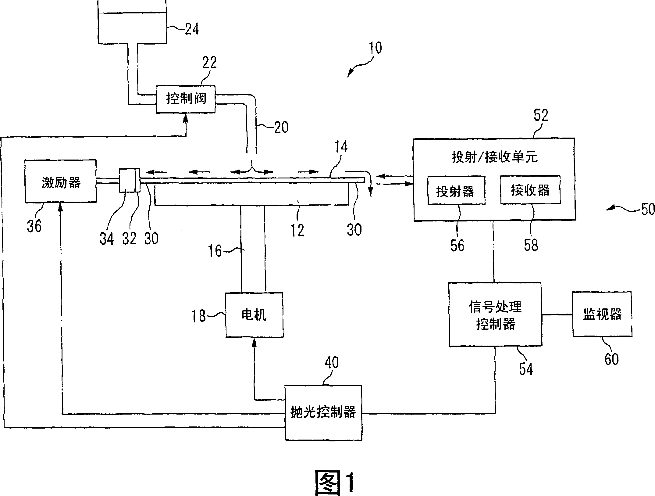
[0083] In FIG. 1 , a substrate peripheral portion polishing apparatus 10 is provided with a rotatable substrate holder 12 . A wafer 14 is held on a substrate holder 12 . The spindle 16 of the substrate holder 12 is connected to a motor 18 . As this motor 18 rotates, the wafer 14 rotates with the substrate holder 12 . A nozzle 20 is arranged above the substrate holder 12 . This nozzle 20 is connected to a water tank 24 via a control valve 22 .

[0084] As a component for polishing the peripheral portion 30 of the wafer 14, a polishing tape 32 is...


PUM

PropertyMeasurementUnit
lengthaaaaaaaaaa
depthaaaaaaaaaa
diameteraaaaaaaaaa

Abstract

A projecting / receiving unit (52) projects a laser light to a peripheral portion (30) and receives the reflected light while a liquid is being fed to a substrate (14) and is flowing on the peripheral portion (30). A signal processing controller (54) processes the electric signal of the reflected light to decide the state of the peripheral portion (30). The state of the peripheral portion being polished is monitored. Moreover, the polish end point is detected. A transmission wave other than the laser light may also be used. The peripheral portion (30) may also be enclosed by a passage forming member thereby to form a passage properly. The peripheral portion can be properly measured even in the situation where the liquid is flowing on the substrate peripheral portion.

Description

technical field [0001] The present invention relates to a substrate peripheral portion measuring device for measuring the state of a substrate peripheral portion. This substrate peripheral portion measuring device belongs to, for example, a semiconductor wafer peripheral portion polishing apparatus, and is used to measure a polishing state of a peripheral portion being polished. Background technique [0002] With the development of miniaturization and high integration of semiconductor devices, the handling of particles becomes more important. One of the major problems in particle handling is dust formation, which is caused by surface roughness generated on the peripheral portion of a semiconductor wafer (or substrate) at the time of manufacturing a semiconductor device. [0003] In the semiconductor device manufacturing process, cracks or a large number of fine needle-like protrusions may be formed in the peripheral portion of the semiconductor wafer, resulting in surface r...

Claims


Application Information

Patent Timeline
Patent Type & Authority Applications(China)
IPC IPC(8): B24B49/12B24B9/00H01L21/304G01B11/30G01N21/956B24B9/06G01N21/95H01L21/306
CPCB24B49/12H01L21/67242B24B9/065H01L21/67075H01L21/67023G01N21/9501G01N29/44B24B9/00G01B11/30H01L21/304
Inventor 多田光男须藤康成市原博文伊藤贤也高桥圭瑞
Owner EBARA CORP
Learn More