Micro nano structure direct-writing device

A technology of micro-nano structure and writing device, which is applied in the direction of nano-structure manufacturing, nanotechnology, nanotechnology, etc., can solve problems such as difficulty, reduce line width, limit application range, etc., achieve spinning voltage reduction, increase utilization rate, reduce The effect of development costs

Inactive Publication Date: 2007-05-23
XIAMEN UNIV
View PDF1 Cites 36 Cited by
  • Summary
  • Abstract
  • Description
  • Claims
  • Application Information

AI Technical Summary

Problems solved by technology

The current material jet printing head is still based on the traditional inkjet printing head technology, the smallest droplet is about 10pl, and th

Method used


Image

  • Micro nano structure direct-writing device

Examples


Embodiment Construction

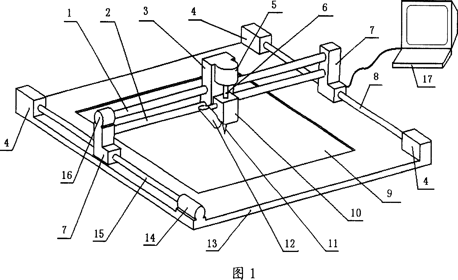
[0018] Referring to Fig. 1, the microprobe control platform of the present invention is provided with Y-direction linear guide rail 1, Y-direction limit slide bar 2, Y-direction slider 3, fixed support 4, Z-direction linear guide rail controller 5, Z-direction linear guide Guide rail 6, X-direction slider 7, X-direction limit slider 8, direct writing area 9, precision flow control and high-voltage electrostatic power supply 10, probe 11, CCD microscope 12, high-speed precision X-Y platform 13, X-direction linear guide rail control Device 14, X-direction linear guide rail 15, Y-direction linear guide rail controller 16 and control computer 17.

[0019] Among them, the X-direction linear guide rail 15 and the Y-direction linear guide rail 1 are driven by the X-direction linear guide rail controller 14 and the Y-direction linear guide rail controller 16 respectively, and control the probe 11 according to the positioning information given by the control computer 17. Precise positi...


PUM


Abstract

The invention relates to a micrometer-nanometer structure writer of polymer material, wherein it is based on near-field static spinning technique, to quickly write adhesive material or macromolecule material, while the minimum diameter/line width is lower than 300nm/20 mum. It has micro probe control platform, integrated high-voltage static power source, flux controller, X-Y platform, probe and CCD microscope; the integrated high-voltage static power source can power the probe, while its anode is connected to probe and cathode is connected to ground; the flux controller is fixed on the micro probe control platform, while it is connected to probe via tube; the probe is used as ejector of material, while it is mounted on micro probe control platform; the microscope is used to detect the spinning process and the writing effect, while it is arranged on micro probe control platform.

Description

technical field [0001] The invention relates to a device for direct writing of micro- and nanoscale materials or patterns based on electrospinning technology, in particular to a direct-writing device for polymer materials with submicron line width. Background technique [0002] In the research and development of micro-nano devices, the integration of nanowires, nanotubes, nanofibers and microstructures (such as microelectrodes) with controllable position, direction and quantity is the key to manufacturing nanodevices such as The key to nanosensors and actuators. The research on nanomaterials has achieved remarkable results and has shown broad commercialization prospects, and has achieved good economic benefits. In view of its special excellent physical and chemical properties, low-dimensional nanomaterials are the basic materials for constructing nanodevices and nanostructures. R&D and development of functional devices. Western countries predict that the industrialization...

Claims


Application Information

Patent Timeline
IPC IPC(8): B82B3/00D01D5/00
Inventor 孙道恒王凌云吴德志林立伟
Owner XIAMEN UNIV
Why Eureka
Try Eureka