Cleanout method after tungsten CMP

A technology for cleaning pipelines and hydrofluoric acid, which is applied in the directions of cleaning methods, cleaning methods and utensils using liquids, chemical instruments and methods, etc., to achieve improved cleanliness and good effects.

Inactive Publication Date: 2007-05-23
SHANGHAI HUA HONG NEC ELECTRONICS
View PDF0 Cites 12 Cited by
  • Summary
  • Abstract
  • Description
  • Claims
  • Application Information

AI Technical Summary

Problems solved by technology

[0005] The technical problem to be solved by the present invention is to provide a cleaning method after tungsten CMP,

Method used


Image

  • Cleanout method after tungsten CMP
  • Cleanout method after tungsten CMP

Examples


Embodiment Construction

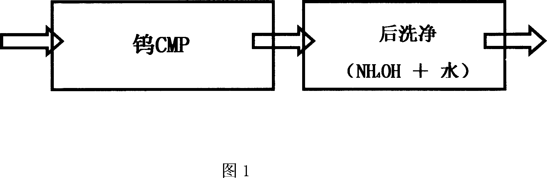
[0011] In the cleaning technology of semiconductor silicon wafers, different chemical solutions are used for cleaning according to the defects of different characteristics, generally alkaline solution and acidic solution are used.

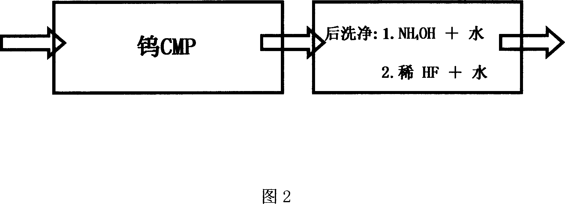
[0012] After the tungsten CMP process is completed, some defects will inevitably occur, including slurry remaining on the surface of the silicon wafer, micro scratches, small pits, and small holes formed on the surface of the silicon wafer. In order to overcome these defects, as shown in Figure 2, the cleaning method after the tungsten CMP of the present invention is that after the tungsten CMP process is completed, the existing ammonia water cleaning process steps are first used to clean the silicon wafer, and after that, use a concentration of <5 % dilute hydrofluoric acid in a short time, generally in the range of 10-20 seconds, to rinse the silicon wafer, then rinse with deionized water and spin dry.

[0013] When performing hydrofluoric acid c...


PUM


Abstract

The invention relates to a method for washing CMP tungsten, wherein after present ammonia clean process, it uses fluohydric acid whose density is lower than 5% to clean silicon sheet; then uses deionized water to wash silicon sheet, dries. The invention can reduce pollution and improve quality.

Description

technical field [0001] The invention relates to a cleaning method of a semiconductor device, in particular to a cleaning method after a chemical mechanical polishing (CMP) process. Background technique [0002] Silicon wafer cleaning is the most important and frequent step in the semiconductor device production process. In order to avoid contamination of semiconductor devices by trace particles and metal impurities and affect the performance and yield of devices, silicon wafers need to be cleaned repeatedly and multiple times in the semiconductor manufacturing process. [0003] In the existing semiconductor manufacturing process, in order to better meet the high requirements of photolithography for planarization, the chemical mechanical polishing process has been widely used in deep submicron technology (<0.25um). Tungsten CMP is mainly used to replace the etch-back of the tungsten layer, which can smooth the particles generated during the deposition of tungsten and even...

Claims


Application Information

Patent Timeline
IPC IPC(8): H01L21/321H01L21/3213H01L21/302H01L21/306B08B3/04B08B3/08
Inventor 陈华伦
Owner SHANGHAI HUA HONG NEC ELECTRONICS
Why Eureka
Try Eureka