
DMOS device and manufacturing method thereof

A manufacturing method and device technology, applied in semiconductor/solid-state device manufacturing, semiconductor devices, electrical components, etc., can solve problems such as peeling of covering layers, old packaging equipment, and metal defects, so as to improve accuracy, ILD layer and metal The effect of tight interface

Active Publication Date: 2014-05-28
CSMC TECH FAB2 CO LTD
View PDF4 Cites 0 Cited by
  • Summary
  • Abstract
  • Description
  • Claims
  • Application Information

AI Technical Summary

Problems solved by technology

[0004] The applicant found in practice that although the above technical solution can clearly identify the gate region and source region of the DMOS device and improve the accuracy of the subsequent wire bonding process, due to the old part of the packaging equipment, the use of Cu with relatively high hardness During wire packaging, the peeling of the cover layer often occurs in the tensile test after packaging. In the die area, the last layer of metal is pulled up, and the source and gate have aluminum peeling. permanent metal defect

Method used


Image

  • DMOS device and manufacturing method thereof
  • DMOS device and manufacturing method thereof
  • DMOS device and manufacturing method thereof

Examples


Embodiment

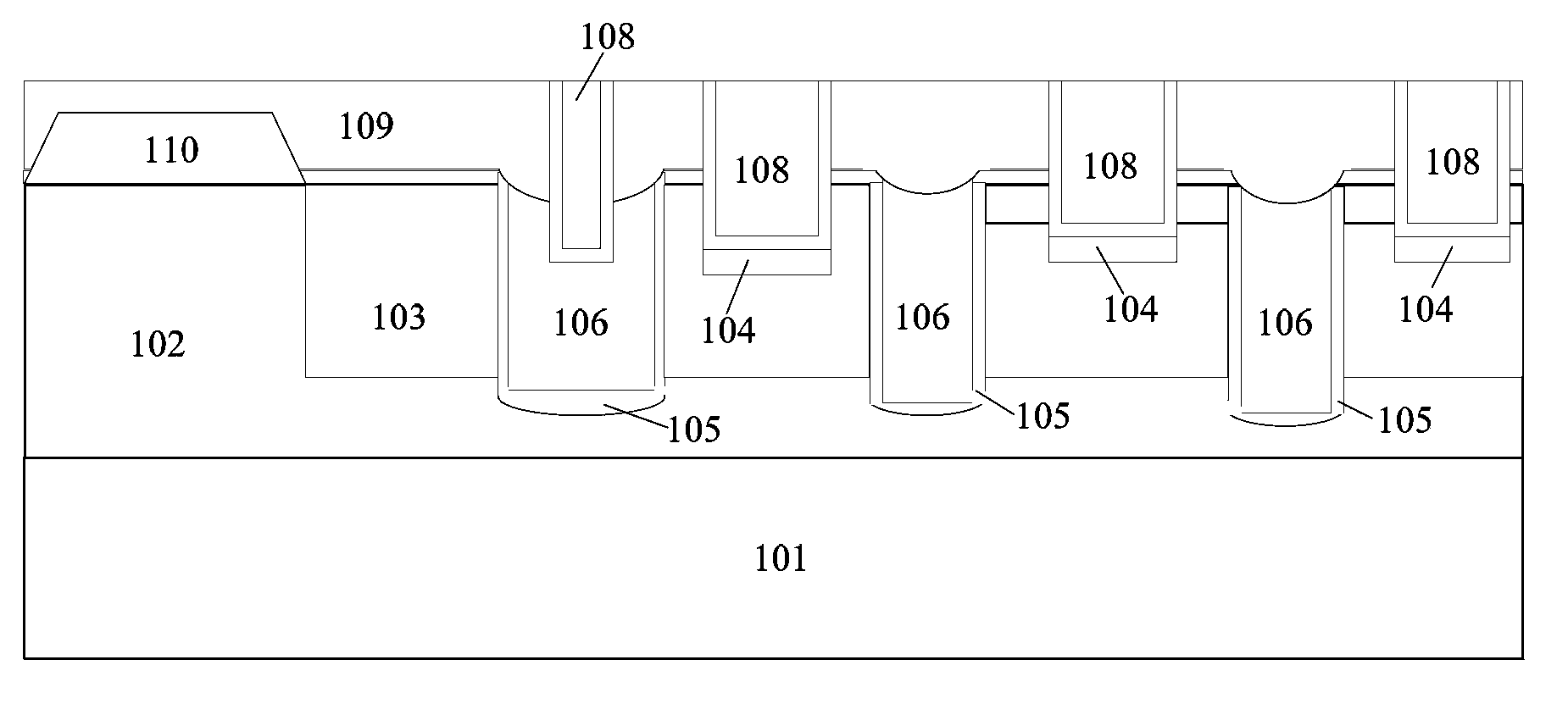
[0044] The cross-sectional view of each step of the DMOS device manufacturing method disclosed in the embodiment of the present invention is as follows image 3 and Figure 4 shown, including the following steps:

[0045]Step 1: provide a substrate, the substrate includes an active region and an interlayer dielectric ILD layer 109 on the surface of the active region, wherein the ILD layer on the surface of the active region has a tungsten plug 108, the ILD The surface of the layer 109 is flush with the surface of the tungsten plug 108;

[0046] It should be noted that the substrate in this embodiment may include semiconductor elements, such as silicon or silicon germanium (SiGe) in single crystal, polycrystalline or amorphous structure, or mixed semiconductor structures, such as silicon carbide, indium antimonide , lead telluride, indium arsenide, indium phosphide, gallium arsenide or gallium antimonide, alloy semiconductors or combinations thereof; also silicon-on-insulator...


PUM


Abstract

The invention discloses a manufacturing method for a DMOS device. The method includes: providing a substrate which includes a source region and an inter-layer dielectric (ILD) layer located on the surface of the source region, wherein the ILD layer located on the surface of the source region is provided with tungsten plugs inside and the surface of the ILD layer is flush with the surfaces of the tungsten plugs; removing the material of the ILD layer for a preset thickness so as to make the ILD layer have a height difference with the surfaces of the tungsten plugs; adopting an EKC solution to rinse for 5-30 minutes at a temperature of 65-70 degrees and adopting isopropyl alcohol to remove the residual EKC solution and filling water for a plurality of times and then spin drying; forming a metal layer on the ILD layer and the surfaces of the tungsten plugs, which have a height difference and beginning a metal interconnection process and forming pressure welding points on the metal layer after the metal interconnection process is completed; and carrying out a low-temperature alloy process and completing the manufacturing process of the DMOS device. The manufacturing method for the DMOS device removes a polymer generated after back etching of the ILD layer through adding of the EKC cleaning step so that the ILD layer is more close to a metal interface and a metal layer formed subsequently is not liable to peel off after packaging.

Description

technical field [0001] The invention belongs to the technical field of semiconductor manufacturing, and in particular relates to a DMOS device and a manufacturing method thereof. Background technique [0002] After the manufacturing process of the semiconductor chip is completed, the silicon wafer that has passed the electrical test needs to be assembled and packaged for a single chip. These processes in the final assembly and packaging are called the back-end process, and the back-end process also includes a packaging and secondary packaging, etc. One-level packaging includes processes such as backside thinning, slicing, racking, and wire bonding. In the wire bonding process, it is necessary to electrically connect the metal pressure point on the chip surface with the inner end of the electrode (also called a post) on the lead frame or on the base. Before this, for DMOS devices, it is necessary to identify the device The gate area and source area of ​​the device, and then...

Claims


Application Information

Patent Timeline
Patent Type & Authority Applications(China)
IPC IPC(8): H01L21/336H01L21/60
CPCH01L29/66734H01L21/02057H01L21/02096
Inventor 杨乐万颖
Owner CSMC TECH FAB2 CO LTD
Learn More