Electroluminescence element and display device using the same

A technology of electroluminescent elements and light-emitting layers, which is applied in the direction of electroluminescent light sources, electrical components, electric light sources, etc., can solve the problems of reduced light displayed, reduced luminous efficiency of EL elements, and inability to extract light from the light-emitting layer, etc., to achieve Effect of improving luminous efficiency

Inactive Publication Date: 2007-05-23
SEIKO INSTR INC
View PDF1 Cites 41 Cited by
  • Summary
  • Abstract
  • Description
  • Claims
  • Application Information

AI Technical Summary

Problems solved by technology

For this reason, light cannot be extracted from the emissive layer, so light is confined in the emissive layer
Therefore, there is a problem that the luminous efficiency of the EL element used for the planar light emitter is lowered
For this reason, there is a problem in that the amount of light extracted for display must be reduced

Method used


Image

  • Electroluminescence element and display device using the same
  • Electroluminescence element and display device using the same
  • Electroluminescence element and display device using the same

Examples


Embodiment 1

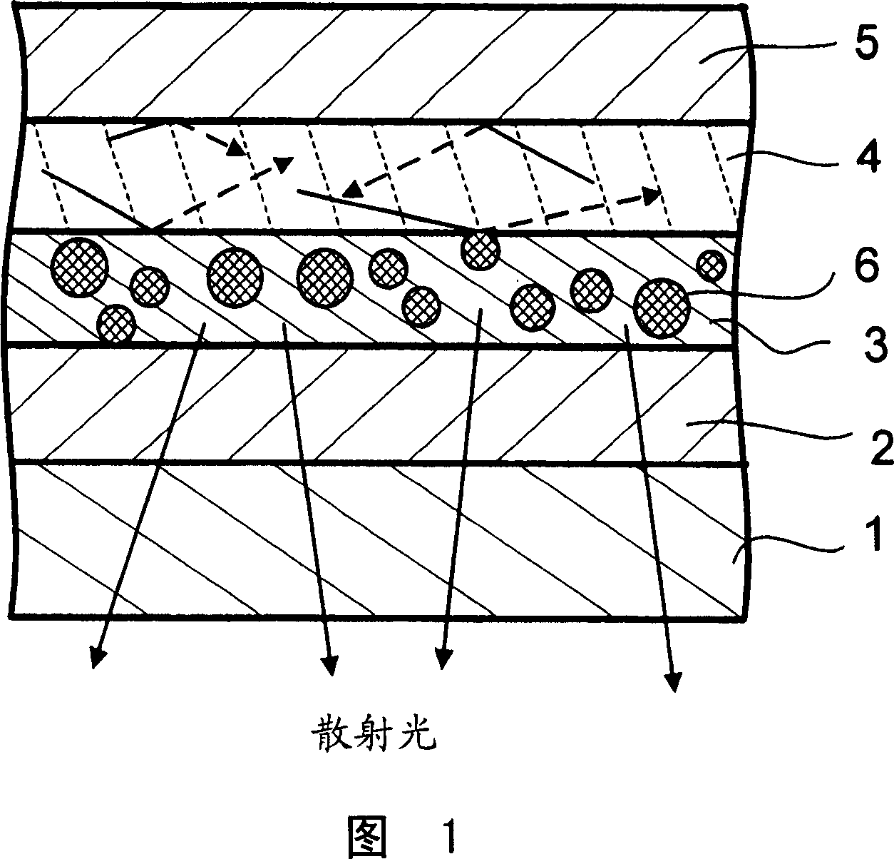
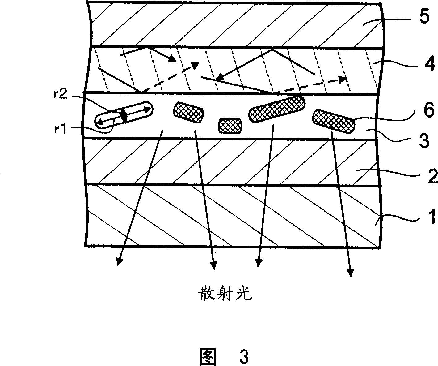
[0050] The EL element according to the present embodiment will be described with reference to FIG. 1 . As shown in FIG. 1 , a transparent first electrode layer 2 is formed on a transparent substrate 1 . Then, a light scattering layer 3 in which metal particles 6 are dispersed in a dielectric material is formed on the first electrode layer 2 . Then, the light emitting layer 4 and the second electrode layer 5 are formed on the light scattering layer 3 . In this embodiment, an EL element used as a flat light emitting panel will be described. This EL element can be used for a lighting device provided in the back of a liquid crystal display device. As shown in FIG. 1, a light scattering layer in which metal particles are dispersed is formed between the first electrode layer and the light emitting layer. For this, light collides with metal particles so that the light can be extracted.

[0051] A voltage is applied between the first electrode layer and the second electrode layer ...

Embodiment 2

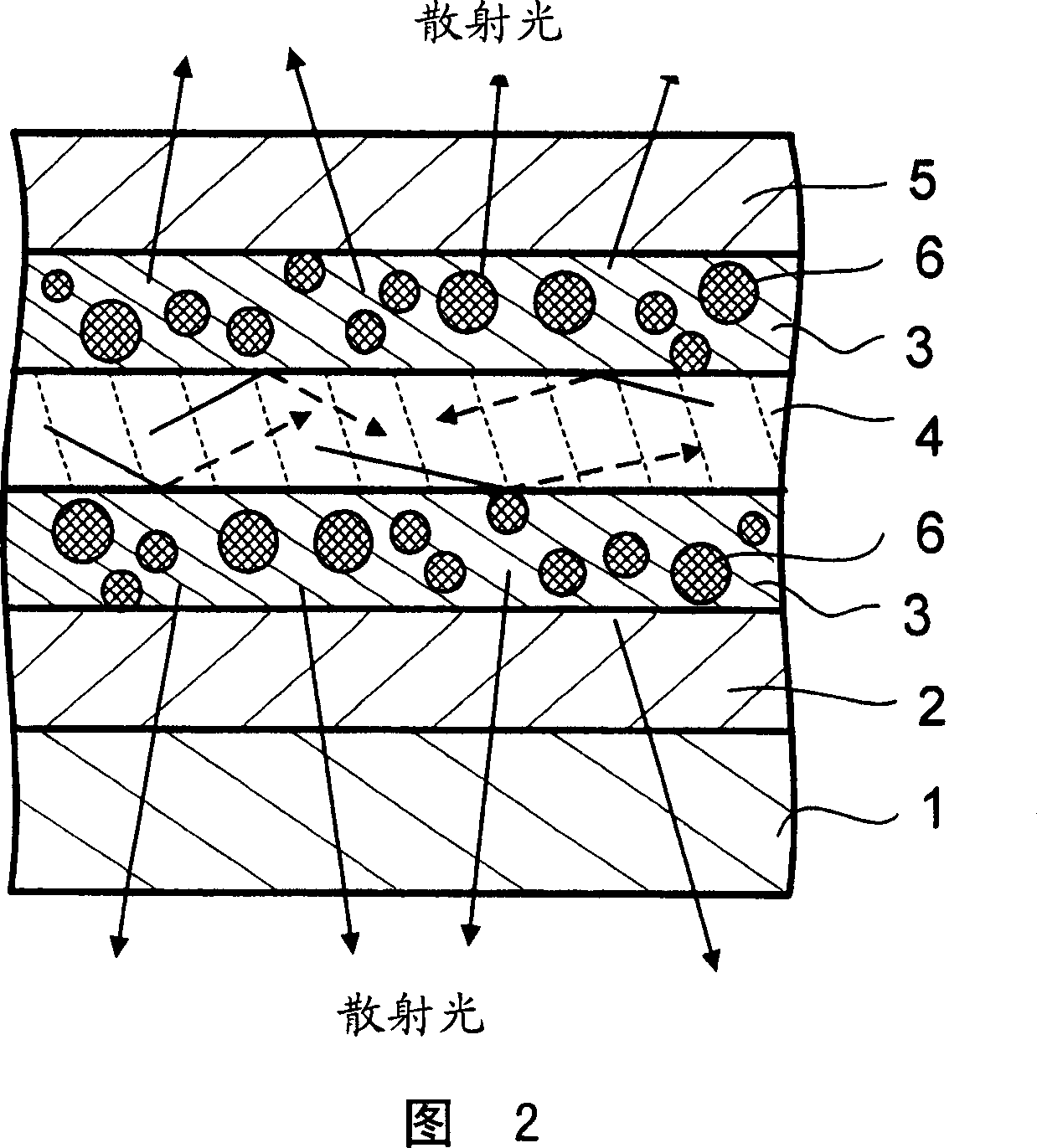
[0068] Fig. 7 is a partial schematic view showing the cross-sectional structure of the EL element according to this embodiment. An important difference between the EL element according to this embodiment and the EL element according to Embodiment 1 is that the light scattering layer 3 is provided not between the first electrode layer and the light emitting layer but on the second electrode layer 5 . Other structures and structural arrangements are the same as those in Embodiment 1, and redundant descriptions are omitted here. In the structure according to this embodiment, an opaque metal electrode is used as the second electrode layer 2 and a transparent electrode layer is used as the second electrode layer 5, so that upper scattered light from FIG. 7 is obtained. The light emitting layer 4 is in contact with the second electrode layer 2 and the second electrode layer 5 . There is thus the advantage that a reduction in the voltage applied to the light-emitting layer 4 or a su...

Embodiment 3

[0070] FIG. 9 is a partial schematic diagram showing a cross section of the EL element according to this embodiment. A structure in which an EL element according to the present invention is used for a display device will be described. Here, an example of an EL element in which a plurality of electrodes spaced apart from each other are formed corresponding to three kinds of light scattering regions will be described. As shown in Figure 9, the first electrode layer 2 is formed on a transparent substrate 1 made of glass or the like, and the first electrode layer 2 is a plurality of spaced strip electrodes extending parallel to the paper plane direction of Figure 9 one of the group. The light scattering layer 3 is formed on the first electrode layer 2 . The light emitting layer 4 is formed on the light scattering layer 3 . The second electrode layer -B 5b , the second electrode layer -G 5g , and the second electrode layer -R 5r spaced apart from each other and provided in strip...


PUM


Abstract

In an EL element including a light emitting layer sandwiched between upper and lower electrodes, of light emitted therefrom, light totally reflected at a light emitting layer interface is not taken out, so there is a problem in that light emission efficiency reduces. Therefore, a light scattering layer in which metal particles are dispersed is provided between an electrode and the light emitting layer. According to such a structure, the light from the light emitting layer can be scattered by the metal particles and taken out, thereby improving the light emission efficiency. When plasmon is excited in the metal particles, light confined in the light emitting layer or each layer adjacent thereto can be used, thereby improving light use efficiency.

Description

technical field [0001] The present invention relates to electroluminescence elements (hereinafter referred to as EL elements) used in planar light emitters, display devices, etc., and more particularly to EL elements in which a light-scattering film is provided near a light-emitting layer to improve luminous efficiency. Background technique [0002] So far, inorganic EL elements including a light emitting layer made of inorganic materials have been known. In recent years, an organic EL element using a low-molecular organic thin film or a polymer organic thin film as a light-emitting layer has been under development. This EL element has the feature that the device is thin and emits light with low power consumption. Therefore, this EL element has been put into practical use as a planar light emitter to illuminate liquid crystal displays. In addition, EL elements for full-color image display devices in which pixels are arranged in a dot matrix have been under research and dev...

Claims


Application Information

Patent Timeline
Patent Type & Authority Applications(China)
IPC IPC(8): H01L51/50H01L51/54H01L27/32H05B33/22
CPCH10K59/38H10K59/877
Inventor 大海学须田正之山本修平杉野谷充千本松茂
Owner SEIKO INSTR INC
Why Eureka
Try Eureka