Encapsulation structure of optical sensing element with micro-packaging area

A packaging structure and light sensing technology, which is applied to color TV parts, TV system parts, electrical components, etc., can solve the problems of large wasted area, waste of area, waste of length, etc.

Inactive Publication Date: 2007-05-30
SIGURD MICROELECTRONICS CORP
View PDF0 Cites 4 Cited by
  • Summary
  • Abstract
  • Description
  • Claims
  • Application Information

AI Technical Summary

Problems solved by technology

However, the center line (a-a') of the photo-sensing area 14 and the center line (bb') of the photo-sensing element 10 often have an offset distance ΔL due to chip manufacturing factors. The packaging method in which the center line (a-a') of the measurement area 14 is positioned with the center of the substrate 12 will cause additional waste of area, that is, a waste of 2×ΔL in length, and the current packaging area is the same in length and width. length, so the wasted area will be (2×ΔL) 2 as much
It can be seen that, if the center point of the light sensing area 14 (image sensing area) of the light sensing element 10 is farther away from the center point of the light sensing element 10, the area to be wasted is larger.
What's more, when the lens base and the lens barrel are to be placed on the package of the light sensor component 10, the traditional assembly method is that the lens barrel corresponds to the center point of the substrate 12, so as to avoid the problem of directionality in the assembly, so the assembled light sensor The module will also face the area of ​​the extra photo-sensing component 10 offset wasted by centering the photo-sensing area 14
This leads to the inability to meet the requirements of a smaller construction area and volume

Method used


Image

  • Encapsulation structure of optical sensing element with micro-packaging area
  • Encapsulation structure of optical sensing element with micro-packaging area
  • Encapsulation structure of optical sensing element with micro-packaging area

Examples


Embodiment Construction

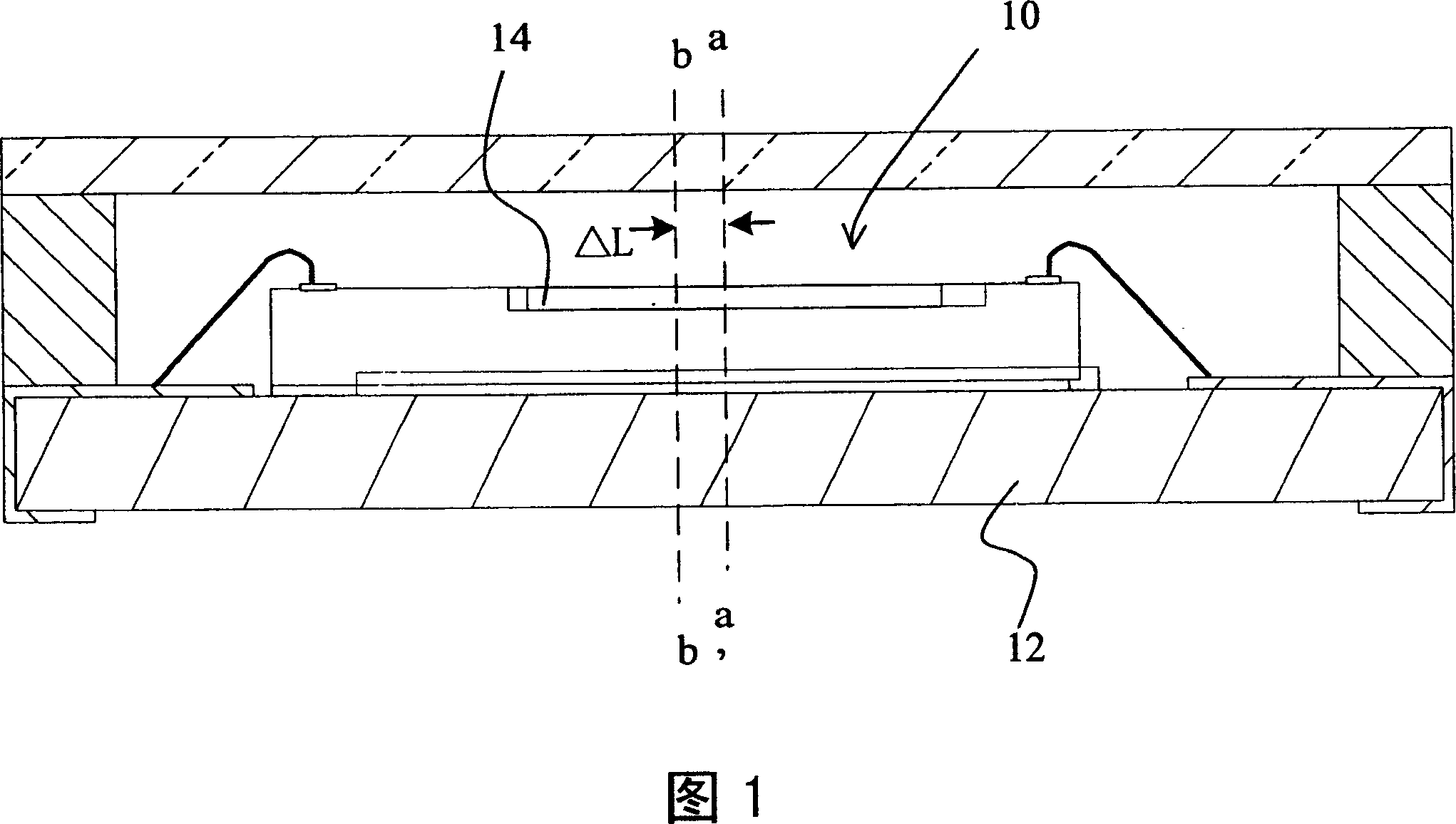
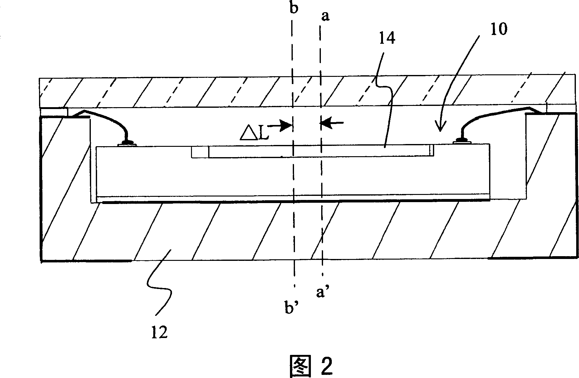
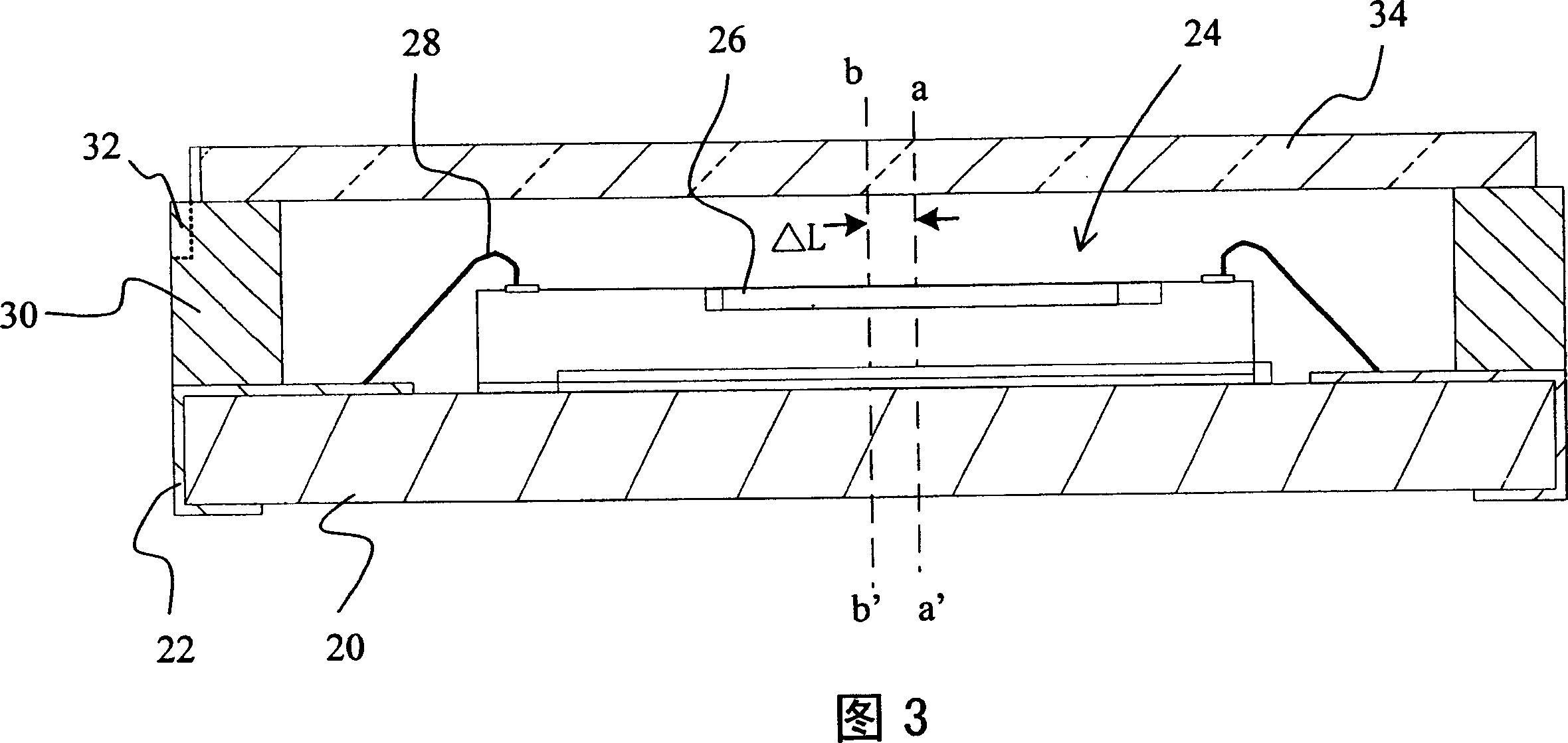
[0050] The invention relates to a packaging structure of a photo-sensing component with a small construction area, which can meet the requirements of light, thin, short and small packaging of a portable photo-sensing component.

[0051] First, please refer to FIG. 3 , which is a schematic diagram of a specific embodiment of the present invention. As shown in the figure, the present invention includes a substrate 20 which may be rectangular or square, and metal wiring 22 is formed at an appropriate position on the substrate 20. In this figure, the metal wiring 22 extends from both sides of the upper surface of the substrate 20 to the lower surface. To facilitate subsequent electrical connection with a PCB board (not shown in the figure) packaging; an optical sensing component 24 located on the substrate 20, which has an optical sensing region 26 and the centerline of the optical sensing component 24 (bb') is located at the center position of the substrate 20 (at this time, the ...


PUM


Abstract

This invention discloses one light sensitive parts package structure with micro structure area, which processes light sense parts sealing by align type of parts central line and baseboard to save the known light sensitive central line as central sealing calibration line area waste to save the whole package area, wherein, it uses proper position to form one card part to add lens cylinder and socket parts for calibration.

Description

technical field [0001] The present invention relates to a packaging structure of a light sensor, in particular to a packaging structure of a light sensing component with a small construction area. Background technique [0002] Driven by the trend of human science and technology, light, thin, short and small portable appeals have become the orientation of the trend of electronic products, and also become an important policy for enterprises to strategize. As a part of the electronic product, light sensing components should also follow this principle. This trend is moving towards the demand for small structure area and volume. [0003] Please refer to FIG. 1 or FIG. 2 , which is a schematic diagram of a package structure of a current CMOS photo-sensing component. It can be seen from the figure that the existing packaging methods are all image-centered, that is, when the light sensing component 10 is positioned on the substrate 12, the center line (a-a') of the light sensing ar...

Claims


Application Information

Patent Timeline
Patent Type & Authority Applications(China)
IPC IPC(8): H01L27/146H04N5/225
Inventor 陈柏宏
Owner SIGURD MICROELECTRONICS CORP
Why Eureka
Try Eureka