
Display apparatus and driving method thereof

A technology for display devices and driving transistors, used in static indicators, instruments, electrical components, etc., to solve problems such as difficulty in realizing large-scale and high-precision image display devices

Inactive Publication Date: 2007-06-06
SONY CORP
View PDF7 Cites 8 Cited by
  • Summary
  • Abstract
  • Description
  • Claims
  • Application Information

AI Technical Summary

Problems solved by technology

The simple matrix method requires a simple image display device structure, but its problem is that it is difficult to realize a large-scale and high-definition image display device

Method used


Image

  • Display apparatus and driving method thereof
  • Display apparatus and driving method thereof
  • Display apparatus and driving method thereof

Examples


Embodiment Construction

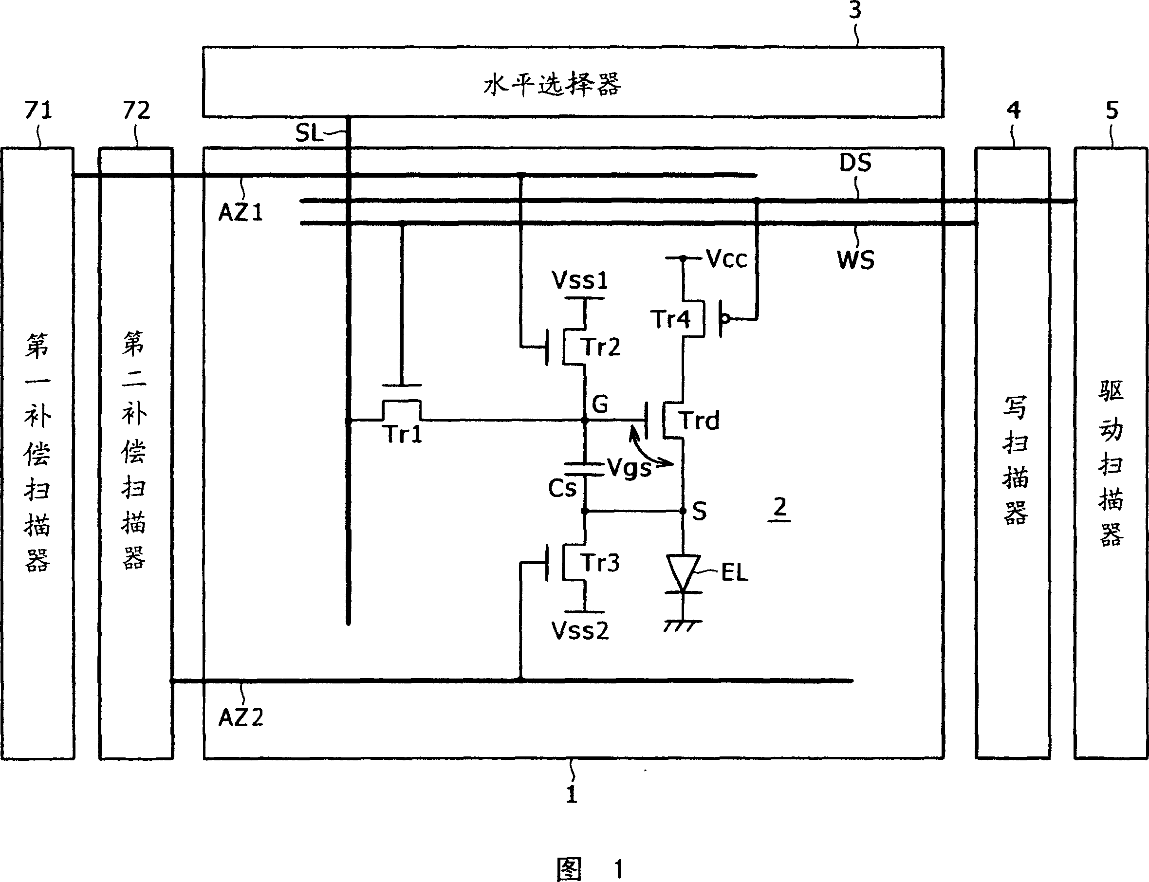
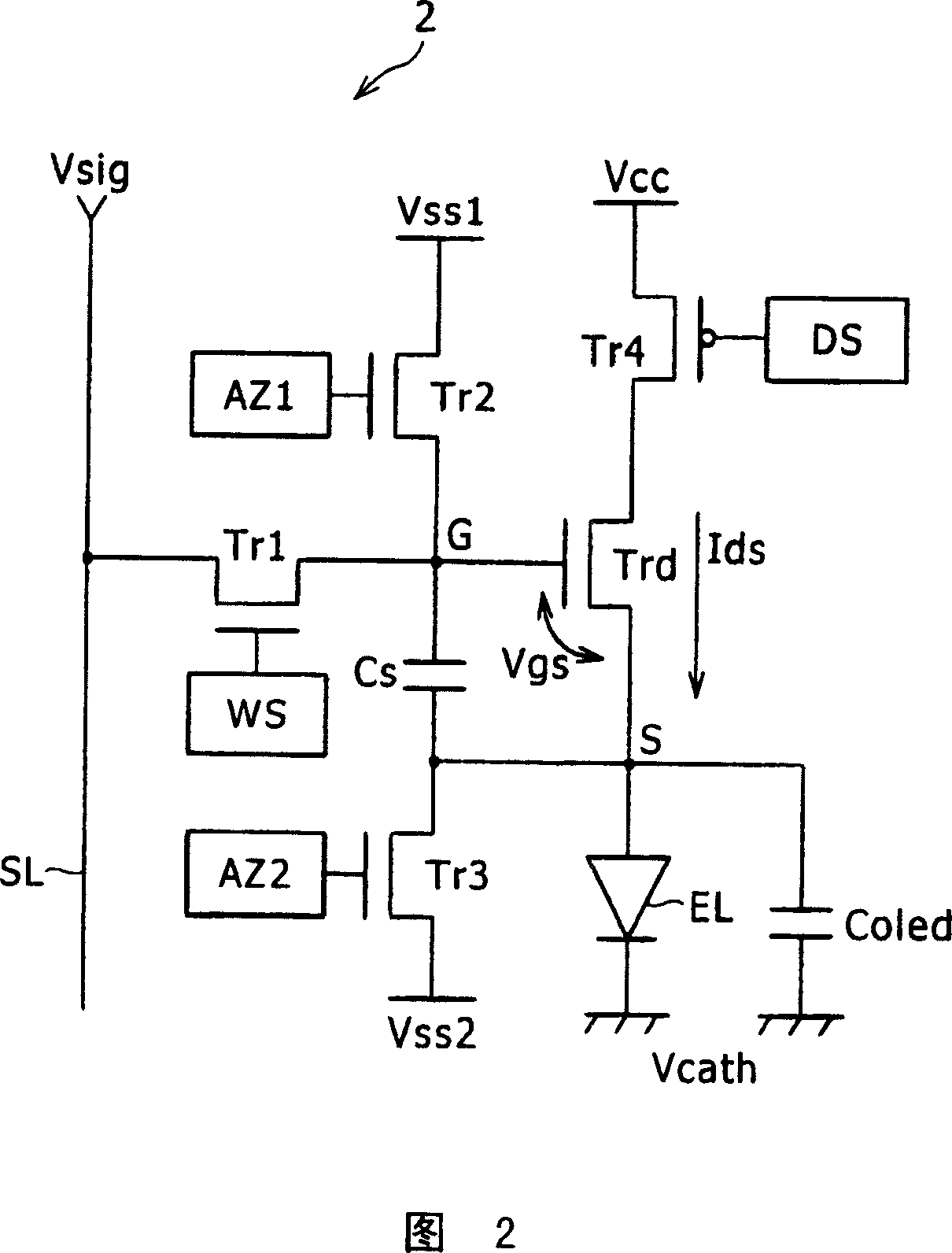
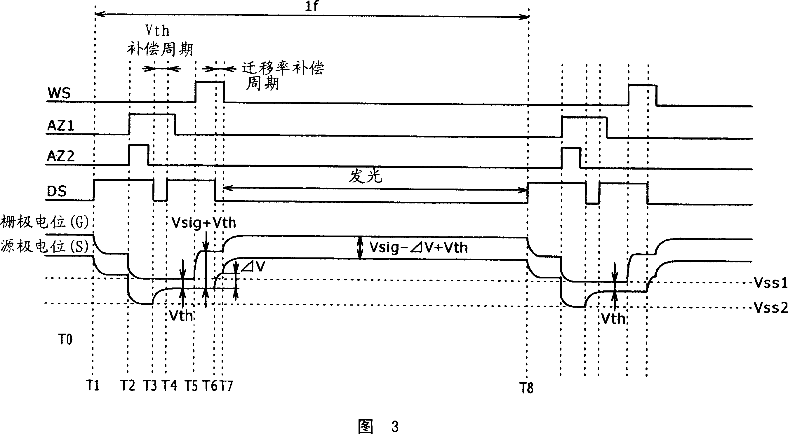
[0068] Preferred embodiments of the present invention will be described in detail below with reference to the accompanying drawings. First, a typical reference implementation of an image display device utilizing the principles of the present invention is explained with reference to FIG. 1 . As shown in the figure, the active matrix display device includes a pixel array unit 1 serving as a main part and its peripheral circuits. The peripheral circuit includes a horizontal selector 3 , a write scanner 4 , a drive scanner 5 , a first compensation scanner 71 and a second compensation scanner 72 . The pixel array unit 1 has pixel circuits 2 arranged to form a matrix. Each pixel circuit 2 is disposed at the intersection of the scan lines WS positioned in the row direction of the matrix and the data signal lines SL positioned in the column direction of the matrix. For easy understanding of the figure, only one pixel circuit 2 is shown in enlarged form. The horizontal selector 3 dr...


PUM


Abstract

Disclosed herein is a display apparatus including a pixel-array unit, a scanner unit and a signal unit. The pixel-array unit has pixels laid out to form a matrix and each provided at an intersection of first and second scanning lines each oriented in a row direction of the matrix and a signal line oriented in a column direction of the matrix. The signal unit provides a video signal to the signal line. The scanner unit sequentially scans the pixels of the matrix in row units by supplying first and second control signals to the first and second scanning lines respectively.

Description

[0001] Cross References to Related Applications [0002] The present invention includes Japanese patent application numbers JP2005-328337, JP2005-344207, and JP2005-372621 filed at the Japan Patent Office on November 14, 2005, November 29, 2005, and December 26, 2005, respectively. related subject matter, the entire contents of which are hereby incorporated by reference. technical field [0003] The present invention relates to a display device that displays an image by driving current to flow to a light emitting device provided in each pixel. To describe in detail, the present invention relates to an image display device in the category of so-called active matrix type, such as an image display device using an insulated gate type field effect transistor in each pixel as a transistor for controlling the amount of current flowing through the A light-emitting device within a pixel, such as a device generally composed of an organic EL device. Background technique [0004] In a...

Claims


Application Information

Patent Timeline
IPC IPC(8): G09G3/30G09G3/32G09G3/20H05B33/18H05B33/14H05B37/02H01L27/32H01L51/50G09F9/33G09G3/3233
Inventor 内野胜秀山下淳一泉岳中村和夫山本哲郎
Owner SONY CORP
Features
  • Generate Ideas
  • Intellectual Property
  • Life Sciences
  • Materials
  • Tech Scout
  • Unparalleled Data Quality
  • Higher Quality Content
  • 60% Fewer Hallucinations
Learn More