

3-D magnetic-field sensor integrated by planes, preparing method and use
A three-dimensional magnetic field and magnetic sensor technology, applied in the direction of the size/direction of the magnetic field, three-component magnetometer, instruments, etc., can solve the problems of high cost, difficulty in ensuring stability and consistency, etc., and achieve high production cost and reduce The effect of volume and stability improvement
- Summary
- Abstract
- Description
- Claims
- Application Information
AI Technical Summary
Problems solved by technology
Method used
Image

Examples
Embodiment 1
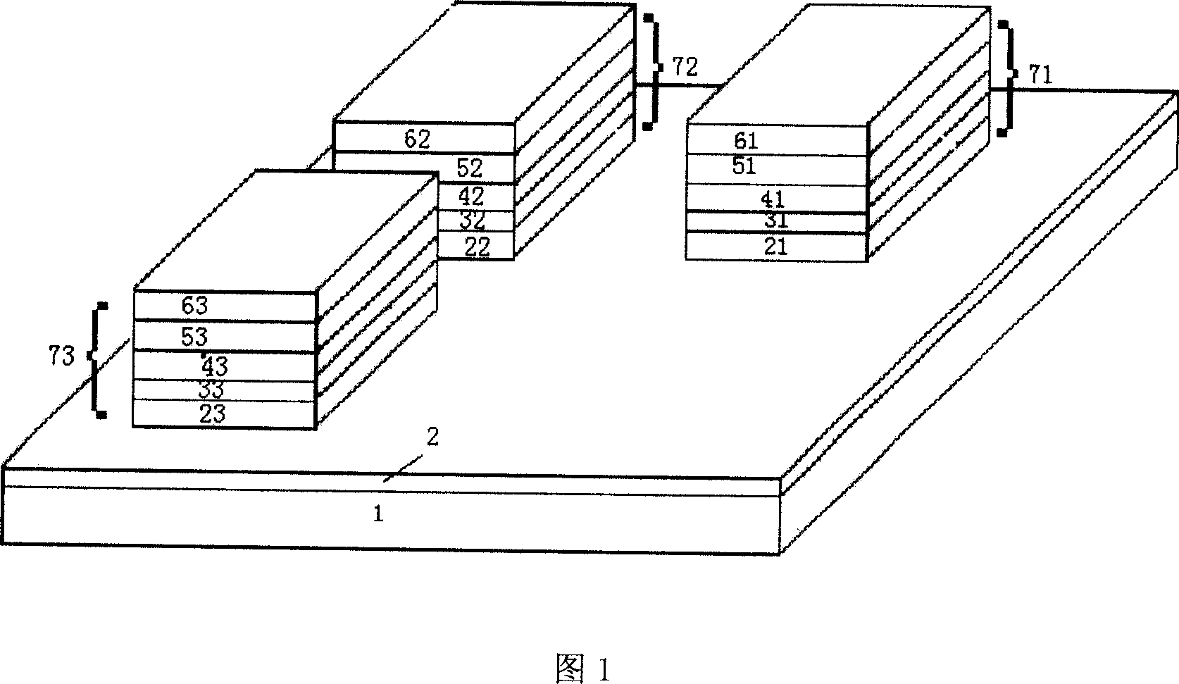
[0042] Embodiment 1, prepare a kind of planar integrated three-dimensional magnetic field sensor with tunnel junction magnetoresistance (TMR) element
[0043] 1), choose a Si-SiO with a thickness of 1mm 2 The substrate is used as the base 1, and the vacuum is better than 5×10 on the magnetron sputtering equipment -5 Pa, the deposition rate is 0.1nm / s, and the argon pressure during deposition is the condition of 0.07Pa, depositing a 5nm Ta buffer layer 2 on the substrate;
[0044] 2) Select a metal mask, which has exactly the same shape as the substrate, and has a 5mm×5mm square hole in the lower left corner. Use the metal mask to shield the substrate and the buffer layer, and use a vacuum better than 5×10 on the magnetron sputtering equipment -5 Pa, the deposition rate is 0.1nm / s, and the argon pressure is the condition of 0.07Pa. On the buffer layer 2, each layer of the first magnetic sensor 72 is deposited successively. At first, the IrMn of 10nm is deposited as the first ...
Embodiment 2
[0053] Embodiment 2, prepare a kind of planar integrated three-dimensional magnetic field sensor with giant magnetoresistance (GMR) element
[0054] 1), choose a Si-SiO with a thickness of 1mm 2 The substrate is used as the base 1, and the vacuum is better than 5×10 on the magnetron sputtering equipment -5 Pa, the deposition rate is 0.1nm / s, and the argon pressure during deposition is the condition of 0.07Pa, depositing a 5nm Ta buffer layer 2 on the substrate;
[0055] 2) Select a metal mask, which has exactly the same shape as the substrate, and has a 3mm×3mm square hole in the lower left corner. Use the metal mask to shield the substrate and the buffer layer, and use a vacuum better than 5×10 on the magnetron sputtering equipment -5 Pa, the deposition rate is 0.1nm / s, and the argon pressure is the condition of 0.07Pa. On the buffer layer 2, each layer of the first magnetic sensor 72 is deposited successively. At first, the IrMn of 10nm is deposited as the first antiferrom...
Embodiment 3~50
[0065] According to the same method as in Example 1 and Example 2, a planar integrated three-dimensional magnetic field sensor was prepared, and the materials and thicknesses of each layer of the magnetic multilayer film are listed in Tables 1-8.
[0066] Table 1, the structure of the magnetic multilayer film for three-dimensional integrated geomagnetic field sensor of the present invention
[0067] Example
3
4
5
6
7
8
Element
Si-SiO 2
Si-SiO 2
Si-SiO 2
Si-SiO 2
Si-SiO 2
Si-SiO 2
thickness
1mm
1mm
1mm
1mm
1mm
1mm
buffer
layer
Element
Ta
Ta
Ta
Ta
Ta
Ta
thickness
3nm
3nm
3nm
3nm
3nm
3nm
First
anti iron
Element
IrMn
Fe-Mn
Pt-Mn
IrMn
Fe-Mn
Fe-Mn
thickness
2nm
2nm
2nm
2nm
2...
PUM
| Property | Measurement | Unit |
|---|---|---|
| Thickness | aaaaa | aaaaa |
| Thickness | aaaaa | aaaaa |
| Thickness | aaaaa | aaaaa |
Abstract
Description
Claims
Application Information