Method for producing field effect transistor and transistor structure made thereof

A field-effect transistor and manufacturing field technology, which is applied in semiconductor/solid-state device manufacturing, semiconductor devices, electrical components, etc., can solve problems such as large area, difficult to control the precise height of silicon channel, and complex channel width correction

Inactive Publication Date: 2007-06-27
KOREA ADVANCED INST OF SCI & TECH
View PDF0 Cites 15 Cited by
  • Summary
  • Abstract
  • Description
  • Claims
  • Application Information

AI Technical Summary

Problems solved by technology

[0019]The device manufactured by this method has the disadvantage that it requires a large area because the channel width of the device must be increased to increase the current value of the device
[0027] This structure has the problem that it is difficult to control the height of the fins compared to the case of using the SOI substrate because the height control layer damaged by the implantation of heavy ions is used to control the height of the fins. Controlling the Precise Height of Silicon Channels
[0035] This structure has the problem that it is difficult to control the precise height of the silicon channel compared to the case of using the SOI substrate, since the height of the fin is controlled using the grooving process
[0036] In addition, there is a problem that it requires a large area because the channel width of the device must be increased to increase the current value of the device
Another problem is that it is complicated to correct the channel width in the device design

Method used


Image

  • Method for producing field effect transistor and transistor structure made thereof
  • Method for producing field effect transistor and transistor structure made thereof
  • Method for producing field effect transistor and transistor structure made thereof

Examples


Embodiment 1

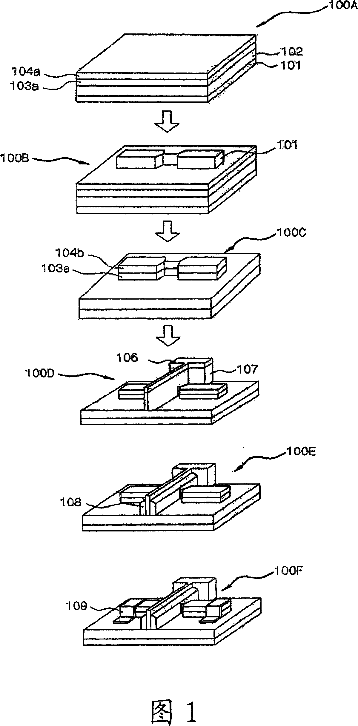
[0059] Figure 4a is a process perspective view sequentially illustrating a method for fabricating a field effect transistor comprising a channel composed of a silicon fin and a silicon body.

[0060] First, an SOI substrate including a silicon substrate 401, a buried oxide film 402, and a silicon thin film 403 formed on the buried insulating film 402 is provided. A hard mask 404 (400A) made of a material that will not be etched in the subsequent anisotropic or isotropic etching of the silicon film 403 is formed on the silicon film 403 (400A).

[0061] In this step, the hard mask 404 may also be formed on the silicon bulk substrate instead of the SOI substrate including the silicon substrate 401 , the buried oxide film 402 and the silicon thin film 403 .

[0062] Then, the silicon thin film 403 is anisotropically etched using the mask pattern 404 as a mask to form a silicon fin 403 in which a channel is to be formed, and a silicon pattern 403a in which a source / drain region is ...

Embodiment 2

[0074] Embodiment 2 of the present invention is the same as Embodiment 1 except that: after performing the step (400C) of etching the silicon body using the active mask 405 to isolate the source / drain regions and the device from each other, A step (400B) of forming silicon fins using the hard mask 400 is performed. Therefore, the drawing showing the second embodiment is omitted here.

[0075] Figure 4b is a cross-sectional view a-a' of a device fabricated by the method shown in Figure 4a.

[0076] It can be seen from Fig. 4b that the silicon fins and the silicon body are used as channels, the orientation of the silicon fins is (110), and the orientation of the silicon body is (100).

[0077] In the case of an NMOS according to one embodiment of the invention, the orientation is (110 ) to compensate for the current reduction caused by the electron mobility in the silicon fins.

[0078] In addition, in the case of PMOS, although the mobility of holes in the (110) orientation ...

Embodiment 3

[0080] 5 is a process cross-sectional view sequentially showing a method for manufacturing a field effect transistor having a channel composed of a silicon fin and a silicon body according to Embodiment 3 of the present invention.

[0081] First, an SOI substrate (500A) including a silicon substrate 501, a buried oxide film 502, and a silicon thin film 503 on the buried oxide film 502 is provided.

[0082] In this step, a silicon bulk substrate may also be used instead of the SOI substrate including the silicon substrate 501 , the buried oxide film 502 and the silicon thin film 503 .

[0083]Then, an oxide film 504 is formed on the silicon thin film 503, and etching and patterning are performed using a mask to form a portion where a silicon fin is to be formed (500B).

[0084] In this step, a material other than an oxide film may also be deposited or grown on the silicon thin film 503 and then etched using a mask.

[0085] Next, silicon fins 503a are formed using selective ep...


PUM


Abstract

This invention discloses a method for manufacturing field effect transistors with channels composed of silicon fins and silicon main bodies and the transistors, in which, the orientation of the fin is defferent from the silicon main body. The method includes the following steps: a, forming a hard mask pattern on a base plate including a Si film, b, etching the Si film to a preset thickness anisotropically using said pattern as the mask so as to form not only Si fins going to form channels and Si pattern with source / drain region but also form a Si main body connecting the fins to form channels, c, using the active mask to etch the Si film partly to isolate the source / drain region and the device and d, growing grid dielectric film on the Si channels and depositing grid material and grid mask on the structure to form a grid region.

Description

technical field [0001] The invention relates to a method of manufacturing a field effect transistor and a transistor structure manufactured by the method. More specifically, the present invention relates to a method of manufacturing a field effect transistor including a channel formed of a silicon fin and a silicon body oriented differently from the silicon fin, and a field effect transistor manufactured by the method. Background technique [0002] Currently, in an attempt to reduce the price of semiconductor devices and improve device performance, the size of semiconductor devices continues to decrease according to Moore's law, thereby enabling high integration of semiconductor IC chips. [0003] However, since the channel length of the semiconductor device is reduced below 100 nm, the potential of the channel in the related art field effect transistor must be controlled not only through the gate region but also through the drain region, so that even when the device is in a...

Claims


Application Information

Patent Timeline
IPC IPC(8): H01L21/336H01L29/78
Inventor 崔梁圭李贤珍
Owner KOREA ADVANCED INST OF SCI & TECH
Why Eureka
Try Eureka