Semiconductor device and method of manufacturing the same

A semiconductor and main body technology, applied in the direction of semiconductor devices, electrical components, nanotechnology, etc., can solve the problems that the characteristics are not optimal, the manufacturing is not very easy, etc., and achieve the effects of easy short circuit, short circuit prevention and high speed

Active Publication Date: 2007-06-27
NXP BV
View PDF1 Cites 2 Cited by
  • Summary
  • Abstract
  • Description
  • Claims
  • Application Information

AI Technical Summary

Problems solved by technology

[0003] The disadvantage of this known device is that the RF (Radio Frequency) characteristics are not yet optimal
Furthermore, the fabrication of the device is not very easy

Method used


Image

  • Semiconductor device and method of manufacturing the same
  • Semiconductor device and method of manufacturing the same
  • Semiconductor device and method of manufacturing the same

Examples


Embodiment approach

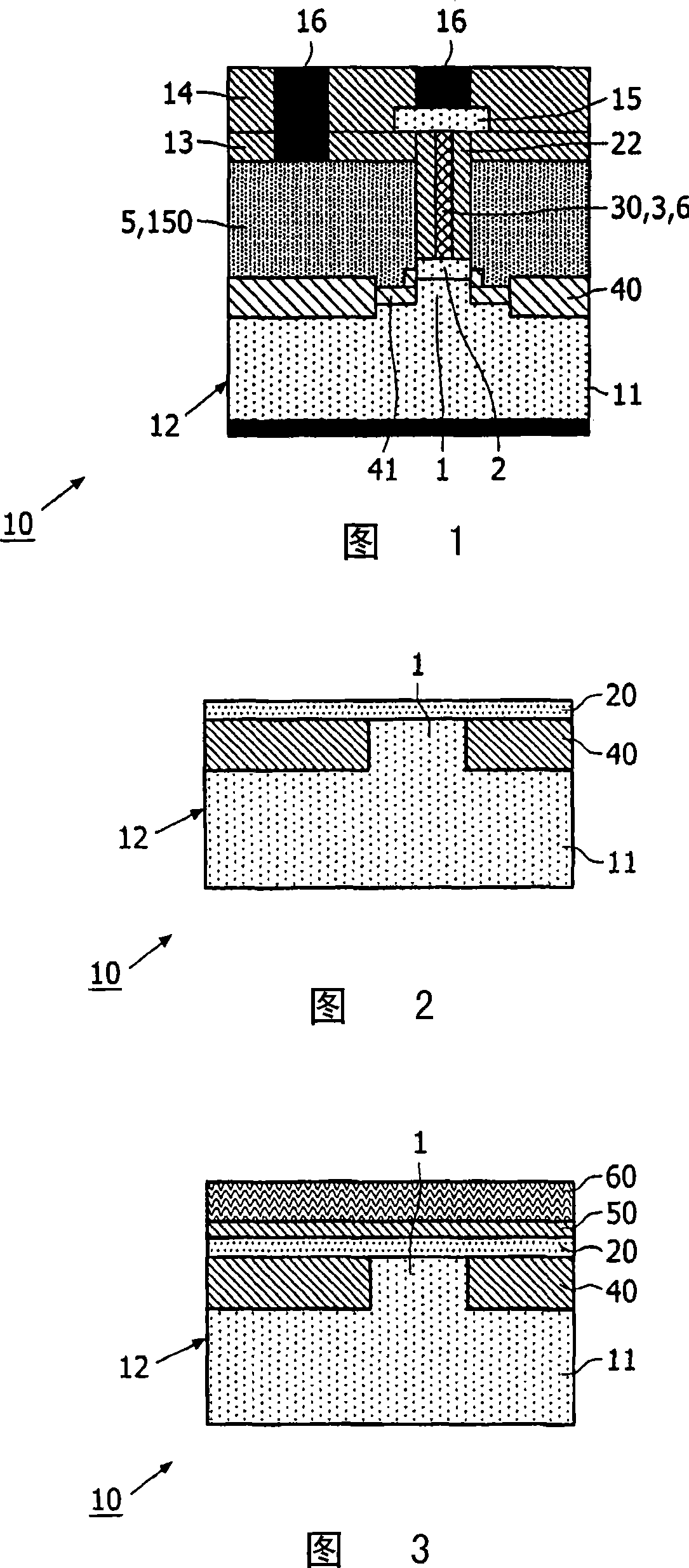
[0027] Located in this case around the nanowires 30 , 3 is a conductive region 150 , which in this case comprises polysilicon and connects directly to the sides of the base region 2 . The conductive region 150 , through which the lightly doped part of the collector region 3 adjoining the base region can be depleted, forms in this case the connection region of the base region 2 and the gate electrode 5 . This is achieved here by choosing the thickness of the conductive region 150 such that it extends beyond the lightly doped portion of the collector region 3 . In addition to being self-aligning, this embodiment is also very compact. This variation can be advantageously used in a device 10 comprising a large number of discrete transistors. Two electrically insulating layers 13 , 14 , for example silicon dioxide, are located on the conductive region 150 . A (large) connection region 15 , in this case polysilicon, is located on the nanowire 30 , this connection region 15 being u...


PUM


Abstract

The invention relates to a semiconductor device (10) with a substrate (11) and a semiconductor body (12) comprising a vertical bipolar transistor with an emitter region, a base region and a collector region (1, 2, 3) of, respectively, a first conductivity type, a second conductivity type opposite to the first conductivity type and the first conductivity type, wherein the collector region (3) comprises a first sub-region (3A) bordering the base region (2) and a second sub-region (3B) bordering the first sub-region (3A) which has a lower doping concentration than the second sub-region (3B), and the transistor is provided with a gate electrode (5) which laterally borders the first sub-region (3A) and by means of which the first sub-region (3A) may be depleted. According to the invention the collector region (3) borders the surface of the semiconductor body (12), while the emitter region (1) is recessed in the semiconductor body (12), and the collector region (3) forms part of a mesa structure (6) formed at the surface of the semiconductor body (12). Such a device (10) has very favorable properties at high frequencies and high voltages and, moreover, is easy to manufacture. In a preferred embodiment the collector (3) comprises a nanowire (30) forming the mesa structure (6).

Description

technical field [0001] The invention relates to a semiconductor device having a substrate and a semiconductor body, the semiconductor device comprising a vertical bipolar transistor having an emitter region of a first conductivity type, a base of a second conductivity type opposite to the first conductivity type a pole region, and a collector region of the first conductivity type, wherein the collector region includes a first subregion adjacent to the base region and a second subregion adjacent to the first subregion, the doping of the first subregion The concentration is lower than the doping concentration of the second sub-region, and the transistor is provided with a gate electrode laterally adjacent to the first sub-region, through which the first sub-region can be depleted. Such a device is well suited for high frequency applications where high voltages are also applied. The collector region has a lightly doped portion, with the result that this portion can be depleted r...

Claims


Application Information

Patent Timeline
Patent Type & Authority Applications(China)
IPC IPC(8): H01L29/08H01L29/06H01L29/423H01L29/737
CPCB82Y10/00H01L29/0804H01L29/7378H01L29/0665H01L29/0821H01L29/0676H01L29/0673Y10S977/936H01L29/70
Inventor G·A·M·胡尔克斯P·阿加瓦尔E·希岑R·J·E·赫廷
Owner NXP BV
Why Eureka
Try Eureka