
Lead frame for direct connected chip packaging

A technology of chip packaging and lead frame, applied in the direction of electrical components, electric solid devices, circuits, etc., can solve the problems of chip circuit damage, large current limit, poor heat dissipation, etc., to reduce the electrical impedance rate, improve Current capacity, heat dissipation capability, cost reduction effect

Inactive Publication Date: 2007-07-04
JCET GROUP CO LTD
View PDF0 Cites 0 Cited by
  • Summary
  • Abstract
  • Description
  • Claims
  • Application Information

AI Technical Summary

Problems solved by technology

Disadvantages are: high electrical impedance, large current limit and poor heat dissipation
[0004] 2. Both the base island and the gold wire soldering pin need to be plated with silver
The disadvantage is: the cost of silver plating is high, and the scrap rate due to poor silver plating is also high
The disadvantage is that the parameters of each operation are limited. A little carelessness will cause damage to the chip surface and internal circuits of the chip, and the parameters need to be re-modified due to different chip thicknesses and different gold wire diameters.

Method used


Image

  • Lead frame for direct connected chip packaging
  • Lead frame for direct connected chip packaging
  • Lead frame for direct connected chip packaging

Examples


Embodiment Construction

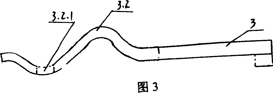
[0017] As shown in FIG. 3 , the present invention is a lead frame for direct connection type chip packaging. The signal guiding lead pin 3.2 of the metal lead frame 3 is made into a spring pin, and the lead pin 3.2 is provided with a connection hole 3.2.1.

[0018] As shown in Figures 4-5, Figures 4-5 show a direct-connected chip packaging structure of the present invention. It consists of a functional chip 1, a conductive or non-conductive glue 2 for connecting the chip and the carrier base island, a metal lead frame 3, and a plastic encapsulant 5 for protection. The functional chip 1 is placed on the carrier base island 3.1 of the metal lead frame 3, the back of the chip 1 and the carrier base island 3.1 are connected by conductive or non-conductive glue 2, and the signal guide pin 3.2 of the metal lead frame 3 is made into a spring Pin, lead pin 3.2 is provided with connection hole 3.2.1, the pin end of lead pin 3.2 is placed on the front of chip 1, and the pin end of lead...


PUM


Abstract

This invention relates to a direct link chip package with leading-line frame, and its characteristic is producing spring feet at the leading line feet (3.2) of the leading line frame (3). The invention can reduce electrical impedance, improving current and heating radiation capacity, lower costs, no need to adjust parameters part, and connecting firmly.

Description

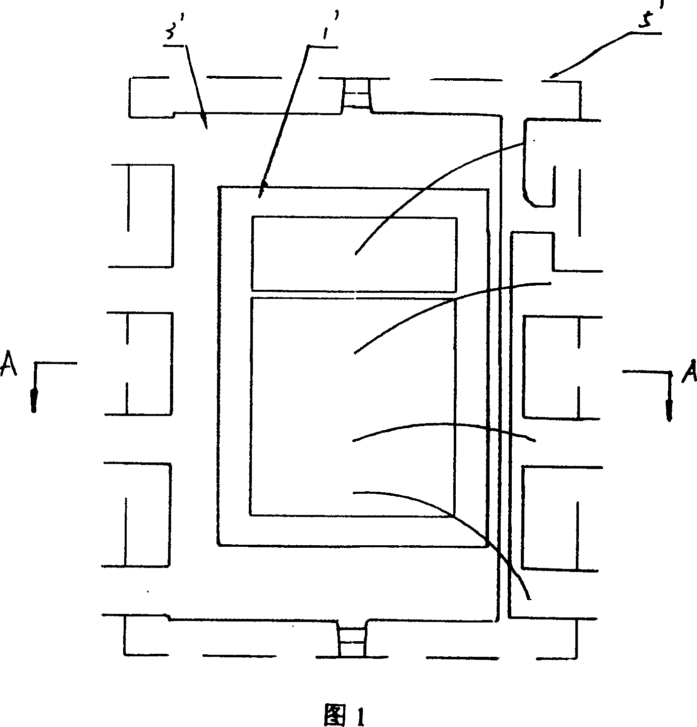
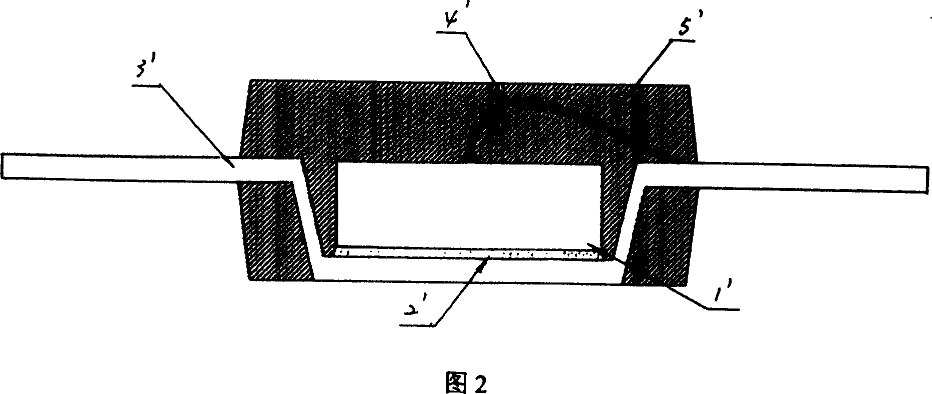
Technical field: [0001] The invention relates to a chip package structure, in particular to a lead frame for direct connection type chip package. It belongs to the technical field of discrete semiconductor devices and integrated circuits. Background technique: [0002] Traditional chip packaging generally uses an indirect lead structure. The packaging structure is shown in Figures 1-2: the functional chip 1' is placed on the carrier base island of the metal lead frame 3', and the conductive or non-conductive glue 2' is used between the back of the chip 1' and the carrier base island of the metal lead frame 3' Connect, the front of the chip 1' and the lead pin of the metal lead frame 3' are welded with a signal guiding gold wire 4', and then the chip 1', the carrier base island of the metal lead frame 3' and the Signal leads gold wire 4' package. It mainly has the following deficiencies: [0003] 1. Gold wire welding is used between the chip and the metal lead frame, ther...

Claims


Application Information

Patent Timeline
Patent Type & Authority Applications(China)
IPC IPC(8): H01L23/495
CPCH01L2224/32245
Inventor 梁志忠刘道明周正伟茅礼卿闻荣福
Owner JCET GROUP CO LTD
Learn More