

CMOS imaging device
A technology of imaging element and element area, which is applied in the field of CMOS imaging element and can solve problems such as unused signal readout
- Summary
- Abstract
- Description
- Claims
- Application Information
AI Technical Summary
Problems solved by technology
Method used
Image

Examples
no. 1 approach
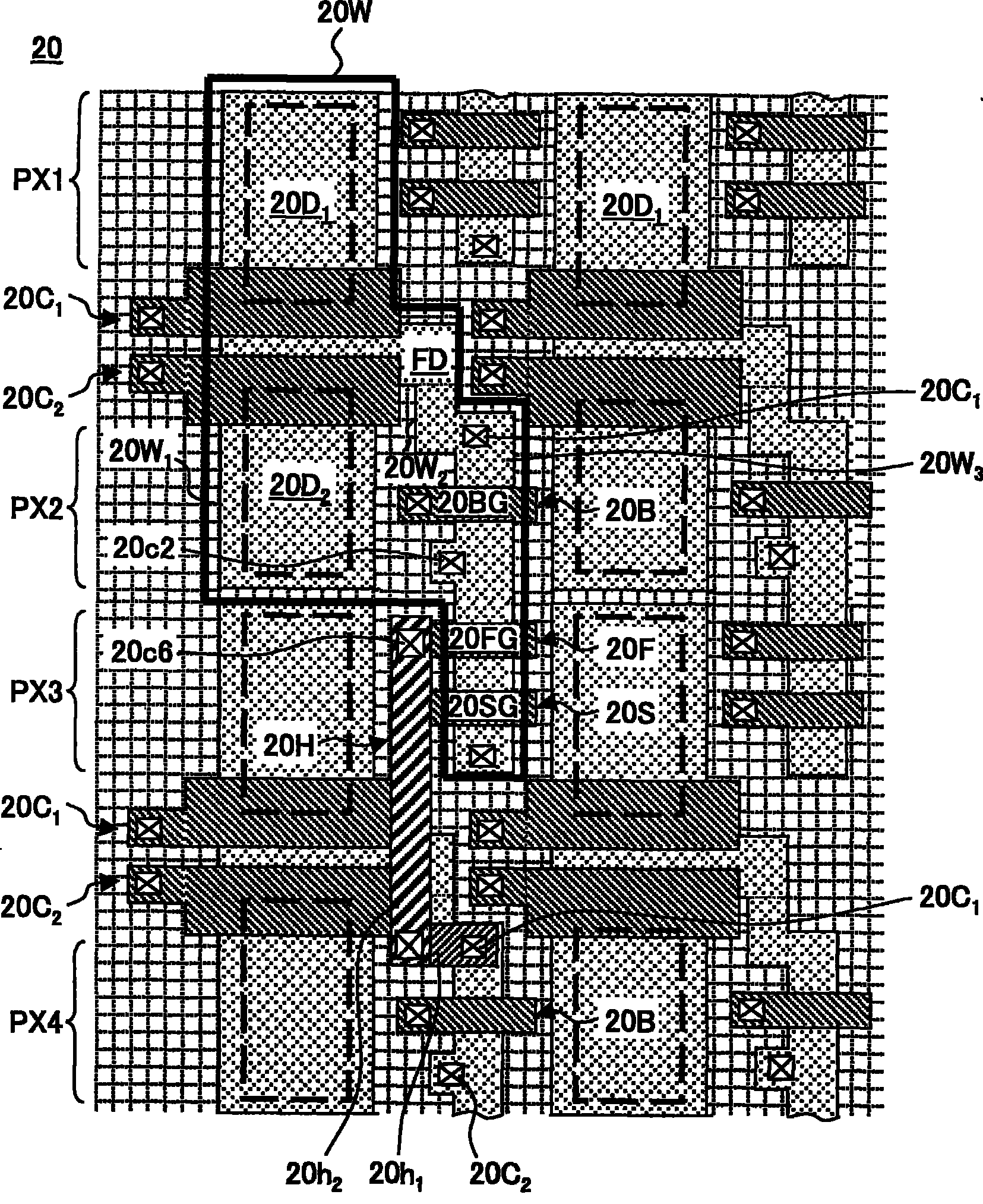
[0120] FIG. 11 shows the layout of the CMOS imaging element 20 according to the first embodiment of the present invention.
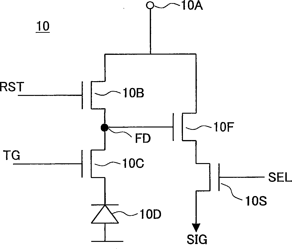
[0121] Referring to FIG. 11 , the CMOS imaging element 20 has the same equivalent circuit as in FIG. 5 and is formed in a single element region 20W divided by element isolation regions 20I on the surface of the silicon substrate.
[0122] More specifically, on the surface of the silicon substrate, an element region portion 20W1 that constitutes a part of the single element region 20W and extends in the column direction (vertical direction in the figure) is divided by the element isolation region 20I. In the portion 20W1, a pixel PX1 corresponding to the CMOS photosensor CMOS1 in FIG. 5 and a pixel PX2 corresponding to the CMOS photosensor CMOS2 in FIG. 5 are formed adjacent to each other in the column direction.
[0123] Therefore, in the element region portion 20W1, the diffusion region 20D1 of the photodiode 10D constituting the CMOS photosensor CMOS1 ...
no. 2 approach
[0174] FIG. 16 shows the structure of a CMOS element 40 according to a second embodiment of the present invention. However, in FIG. 16 , the same reference numerals are assigned to the parts corresponding to the parts described above, and the description thereof will be omitted.
[0175] Referring to FIG. 16, in the present embodiment, the element region portion 20W1 is formed as a band-shaped region continuously extending in the column direction on the surface of the silicon substrate. In the structure of FIG. A p-type well 20PW is formed between the aforementioned pixel PX2 separated by 201 and its adjacent pixel PX3 in the column direction.
[0176] FIG. 17 shows a sectional view along line A-B of FIG. 16 .
[0177] Referring to FIG. 17 , between the diffusion region 20D2 constituting the photodiode PD in the above-mentioned pixel PX2 and the diffusion region 20D1 constituting the photodiode PD in the above-mentioned pixel PX3 , an acceleration voltage of 150 keV was first...
no. 3 approach
[0180] FIG. 18 is a plan view showing the layout of a CMOS imaging element 60 according to a third embodiment of the present invention. However, in the drawings, the same reference numerals are assigned to the parts corresponding to the parts described above, and the description thereof will be omitted.
[0181] Referring to FIG. 18 , in this embodiment, the gate length of the reset transistor 20B is set to be larger than that of other transistors, such as the transfer gate transistors 20C1 and 20C2 , the readout transistor 20F, or the selection transistor 20S. A value of 0.9 μm. Furthermore, as a result of such an increase in the gate length, in the element region of the reset transistor 20B having an enlarged area, ion implantation dedicated to the reset transistor is performed to control the threshold, and the threshold voltage of the transistor 20B is lowered to about 0.1V. For example, in the above-mentioned reset transistor 20B, in the region directly under the above-me...
PUM
| Property | Measurement | Unit |
|---|---|---|
| Thickness | aaaaa | aaaaa |
| Thickness | aaaaa | aaaaa |
| Film thickness | aaaaa | aaaaa |
Abstract
Description
Claims
Application Information