Growth method of graphene

a growth method and graphene technology, applied in the direction of crystal growth process, polycrystalline material growth, chemically reactive gas, etc., can solve the problems of reducing the property of graphene, slow growth rate, destructive and high-cost process, etc., to achieve slow growth rate, high quality, and slow growth rate of graphene

Active Publication Date: 2018-07-10
SHANGHAI INST OF MICROSYSTEM & INFORMATION TECH CHINESE ACAD OF SCI
View PDF0 Cites 0 Cited by
  • Summary
  • Abstract
  • Description
  • Claims
  • Application Information

AI Technical Summary

Benefits of technology

[0007]In view of the above disadvantages in the prior art, the object of the present invention is to provide a growth method of graphene, to solve the problems of slow growth rate of graphene grown on a surface of an insulating substrate surface, low quality of graphene, small single crystalline domain, and high defect density in the prior art.
[0025]From the above, the growth method of graphene of the present invention has the following beneficial effects: by a catalytic manner of introducing catalytic element in the present invention, a high quality graphene is rapidly grown on the insulating substrate. During the process of growing graphene on the insulating substrate, since the substrate lacks of catalysis, the growth rate of the graphene is very slow, and a large amount of defects may be introduced in the crystal lattice of the graphene; in the meanwhile, because of slow growth rate, high nucleation density, the crystalline domains of graphene of the eventually obtained graphene thin film is quite small. By introducing gaseous catalytic element, the catalytic atoms would adsorb around the edge of the graphene in the growth process, to form a chemical bond weaker than carbon-carbon bond; the catalytic atoms adsorbing around the edge of the graphene enables to continue bonding with an active carbon group for capturing an active group, and a transposition between the active atoms and the catalytic atoms is realized by metathesis to achieve the growth of graphene. In the process, the total result is that a potential barrier for an active carbon group bonding with a graphene is reduced by the catalytic atoms, so that the growth rate of the graphene can be greatly improved under the same growth temperature. In the meanwhile, because of the existence of catalytic atoms, the probability of the active carbon group being relaxation to an optimum location becomes large, and the introduced defect density in the growth process is reduced. As such, the gaseous catalytic element not only improves the growth rate of the graphene, but also reduces the defect density of graphene. The growth method of the present invention enables to grow high quality graphene thin film on the insulating substrate, and to avoid the transition process of the graphene; the growth method of the present invention also features relative high growth rate of the graphene, which helps not only improving the production yield of the graphene, but also greatly reducing the growth cost of the graphene, and thus the mass production can be facilitated; the graphene grown by the present invention may be applied in the field of novel graphene electronic devices, graphene transparent conducting film, transparent conducting coating and the like.

Problems solved by technology

The transfer process of graphene itself is a complicated, destructive and high-cost process, which is extremely detrimental to the large-scale mass production; in the meanwhile, it is inescapable to introduce defects and impurities in the transfer process, which greatly reduces the property of the graphene.
Since the substrate lacks of catalytic function, the graphene grown on insulating substrate features slow growth rate, requires relative longer growth time and the obtained graphene has poor quality.
However, the graphene prepared by this method fails to completely cover the hBN substrate, and the thickness control is difficult.
The article “Direct graphene growth on insulator” by G. Lippert et al. has proposed a growth method of graphene on mica surface by MBE method, but the obtained graphene is of poor quality.
The article “Catalyst-free growth of nanographene film on various substrates” by Zhang Lianchang et al. has reported a growth method of nanographene on various substrates by PECVD method, in which the growth duration is generally 2˜5 hours, and the prepared graphene is of nano-sized graphene domains, with the result of poor quality.

Method used


Image

  • Growth method of graphene
  • Growth method of graphene
  • Growth method of graphene

Examples


embodiment 1

[0038]

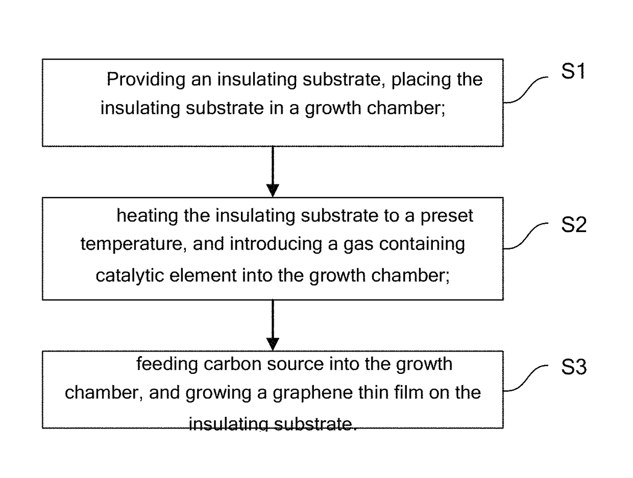
[0039]Firstly perform step S1: providing an insulating substrate, placing the insulating substrate in a growth chamber.

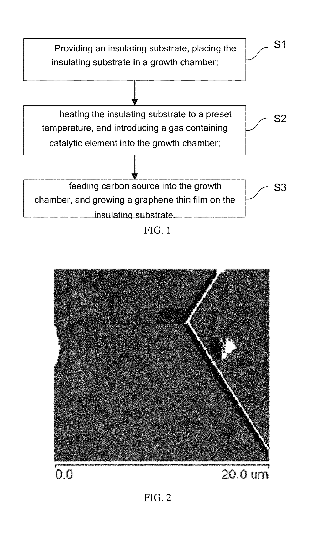
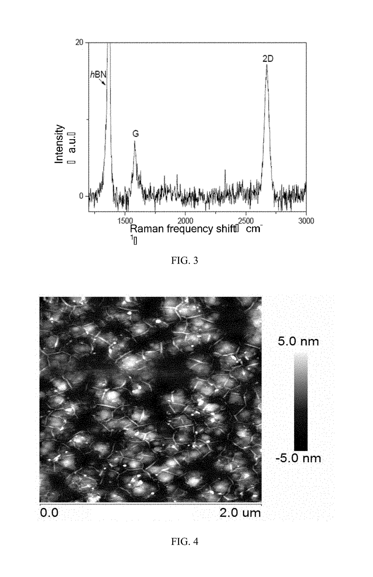
[0040]Specifically, the insulating substrate may be sapphire, silicon carbide, quartz, hexagonal boron nitride, cubic boron nitride, strontium titanate or glass, or the like. In the present invention, the insulating substrate is preferably hexagonal boron nitride (hBN), and the preparation method thereof is that: taking a hexagonal boron nitride single crystal as a raw material, mechanically stripping a silicon substrate with a silicon dioxide layer on an upper surface (silicon dioxide / silicon substrate) to obtain a hexagonal boron nitride layer with a fresh cleavage plane, so as to form a hexagonal boron nitride / silicon dioxide / silicon substrate. The hexagonal boron nitride thin film has a similar crystal structure with the graphene, and has better insulativity, thermal conductivity as well as chemical stability, with the result that when growing the graphene...

embodiment 2

[0059]

[0060]In the present embodiment, the graphene thin film is grown by the low pressure chemical vapor deposition method.

[0061]Firstly perform step S1: providing an insulating substrate, placing the insulating substrate in a growth chamber.

[0062]Specifically, a sapphire substrate is used as the insulating substrate. The sapphire substrate is firstly washed, and then is placed in a tube furnace. In the present embodiment, the manner ii) introducing catalytic element in the first embodiment is adopted, and thus in the present step, a compacted pellet of nano-iron powder is together placed in the tube furnace, and hydrogen-argon gas mixture is fed. Wherein, the flow velocity of the hydrogen-argon gas mixture is preferably 300 sccm, the volume ratio of the hydrogen and the argon is preferably 1:2.

[0063]Next, perform step S2: heating the insulating substrate to a preset temperature, and introducing a gas containing catalytic element into the growth chamber.

[0064]Specifically, the temp...


PUM

PropertyMeasurementUnit
crystalline domain sizeaaaaaaaaaa
temperatureaaaaaaaaaa

Abstract

The present invention provides a growth method of grapheme, which at least comprises the following steps: S1: providing an insulating substrate, placing the insulating substrate in a growth chamber; S2: heating the insulating substrate to a preset temperature, and introducing a gas containing catalytic element into the growth chamber; S3: feeding carbon source into the growth chamber and growing a graphene thin film on the insulating substrate. The present invention adopts a catalytic manner of introducing catalytic element, and rapid grows a high quality graphene on the insulating substrate, which avoids the transition process of the graphene, enables to improve the production yield of the graphene, reduces the growth cost of the graphene, and thus the mass production can be facilitated. The graphene grown by the present invention may be applied in the field of novel graphene electronic devices, graphene transparent conducting film, transparent conducting coating and the like.

Description

BACKGROUND OF THE PRESENT INVENTIONField of Invention[0001]The present invention belongs to the field of low-dimensional material and advanced material, and relates to a growth method of graphene.Description of Related Arts[0002]Graphene was discovered by Geim et al. of the Britain's University of Manchester in 2004. Graphene has various superior natures, comprising thinnest thickness, strongest lattice, high transmittance for visible light, high thermal conductivity, high hardness, high electronic mobility, zero effective mass , ballistic transport at room temperature and high tolerance of current density six orders higher than that of copper, and the like, with the result of showing huge utilization potentiality in the field of the next generation of transistor, transparent conducting film, sensor and the like.[0003]Currently, the popular preparation methods of graphene include: micromechanical cleavage, pyrolytic silicon carbide (SiC), chemical vapor deposition (CVD) on a transit...

Claims


Application Information

Patent Timeline
Patent Type & Authority Patents(United States)
IPC IPC(8): C30B25/04C23C14/06C23C14/28C30B25/20C23C16/26C30B29/02C23C16/50C30B23/02
CPCC30B25/205C23C14/0605C23C14/28C30B29/02C23C16/50C30B23/025C23C16/26C30B29/60
Inventor WANG, HAOMINTANG, SHUJIELU, GUANGYUANWU, TIANRUJIANG, DADING, GUQIAOZHANG, XUEFUXIE, HONGXIE, XIAOMINGJIANG, MIANHENG
Owner SHANGHAI INST OF MICROSYSTEM & INFORMATION TECH CHINESE ACAD OF SCI
Why Eureka
Try Eureka