
Aluminum nanowire arrays and methods of preparation and use thereof

a technology of aluminum nanowires and arrays, which is applied in the field of aluminum nanowire arrays, can solve the problems of affecting the quality of aluminum nanowires, etc., and achieves the effects of low cost, large-scale production, and high tunability of array geometry

Inactive Publication Date: 2018-07-17
BOSTON COLLEGE
View PDF4 Cites 0 Cited by
  • Summary
  • Abstract
  • Description
  • Claims
  • Application Information

AI Technical Summary

Benefits of technology

Enables the production of metal nanowire arrays with tunable geometry and dimensions suitable for advanced applications in energy conversion, material deposition, sensing, and computation, while avoiding clustering issues and enhancing optical and electronic properties.

Problems solved by technology

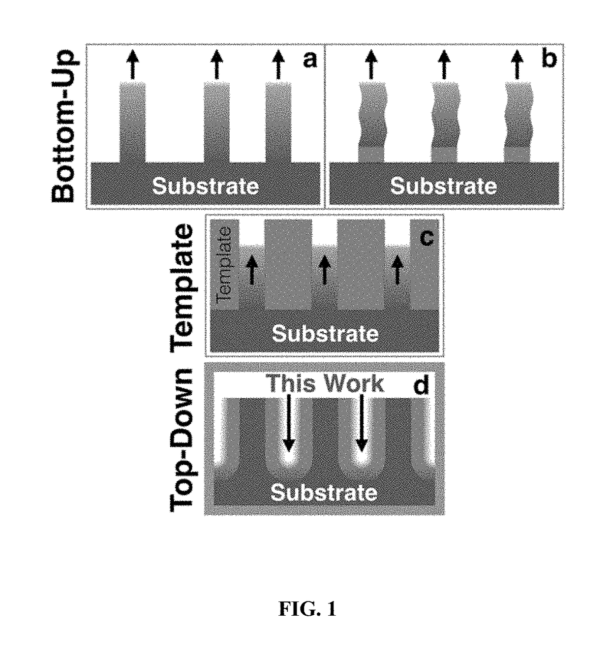
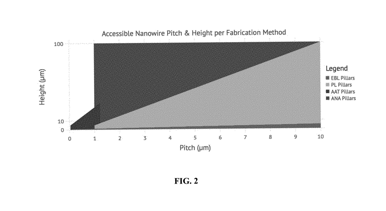
Currently, only a limited range of nanowire heights and array pitches can be produced in ordered arrays using metallic materials.
A notable drawback of the present fabrication processes is that only certain dimensions can be accessed.
If the aspect ratio of the wires becomes too large they are likely to cluster due to van der Waals' interactions, losing their freestanding nature.
This clustering inhibits many material deposition processes from conformally coating the wires, limiting application of the nanowire array to core-shell and nanocoax architectures.

Method used


Image

  • Aluminum nanowire arrays and methods of preparation and use thereof
  • Aluminum nanowire arrays and methods of preparation and use thereof
  • Aluminum nanowire arrays and methods of preparation and use thereof

Examples


example 1

Field Enhancement

[0074]A major application of metal nanostructures is enhancement of the electric field from radiation incident on the structure. In sensors this field enhancement improves the signal strength by enhancing interactions between the radiation and the target species that is in proximity of the nanostructure (e.g. SERS, SPR). In solar cells this field enhancement improves the absorption of the radiation by the solar absorber (e.g. a semiconductor or dye molecule).

[0075]There are two mechanisms for field enhancement with metal nanostructures: geometric confinement of electric field lines at sharp edges and excitation of plasmonic resonances. The former is relevant when the dispersion relation of surface plasmon polaritons (SPPs) is photonic in nature, nearly matching the light line as shown for Al in vacuum from 0 to 6 eV in FIG. 3. In this regime, the metal acts as a perfect electrical conductor (PEC), the electric field has negligible penetration into the metal, and the...

example 2

Al Nanowire Results

Method 1

[0096]Shown in FIG. 11 below is an AAT with a Si pillar embedded into the template, and the corresponding Al nanowire that formed as a result of the Si pillar preventing the nucleation of a pore at that site. An SEM of the Si pillar stamp is shown in FIG. 9.

Method 2

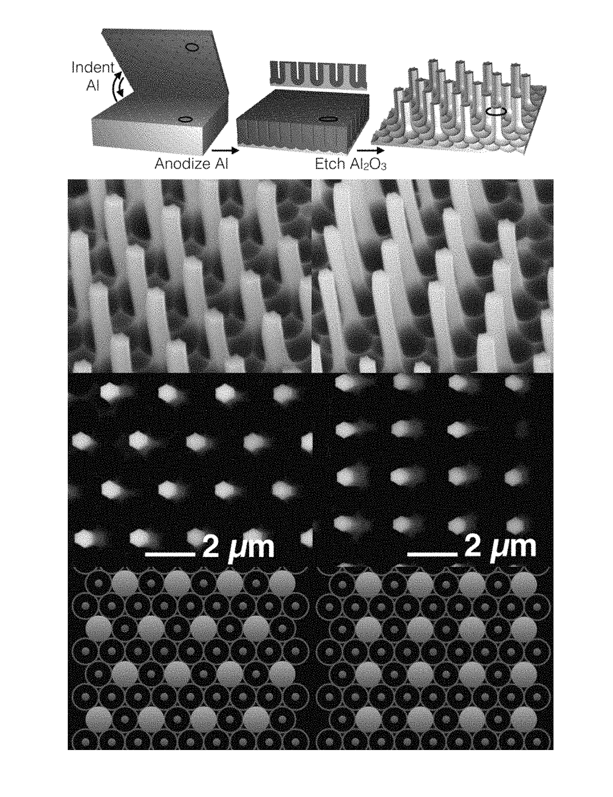
[0097]As shown in FIG. 12 below, it was found that Al nanowires only formed (under anodization conditions for 1.2 μm pore-to-pore pitch) when the diameter of the Ni posts used to indent the Al surface was ≤400 nm. See the SEMs in FIG. 3 for higher aspect ratio Al nanowires fabricated via this process.

example 3

Al Nanowire Array Fabrication

[0098]Ni posts were used to imprint the Al surface with an array of indents. Ni was chosen because of its hardness and compatibility with an electron-beam lithography (EBL) technique for fabricating post arrays. The use of EBL allowed Ni posts to be left out of certain lattice sites in the array, such that after imprinting the Al there would be missing indents at certain lattice sites of the indent array. This prevented the Al from anodizing at the sites of the missing indents. As shown in FIG. 15, there is apparently a maximum indent diameter for which pores selectively nucleate at indented sites and not sites missing an indent. FIG. 16 shows photographs of the experimental setup used in the fabrication of Ni posts and Al nanowires.

[0099]Stamp preparation: To produce the stamp, glass slides 16 mm×15 mm were piranha cleaned and then coated with 50 nm of Ni with a Sharon electron beam deposition system. HMDS (VLSI grade 0.1 μm filtered from Ultra Pure Sol...


PUM

PropertyMeasurementUnit
heightaaaaaaaaaa
heightaaaaaaaaaa
temperaturesaaaaaaaaaa

Abstract

The invention provides a novel, template-free process for the fabrication of metal nanowires of novel dimensions. The unconventional method produces highly ordered and freestanding aluminum nanowire arrays.

Description

PRIORITY CLAIMS AND RELATED APPLICATIONS[0001]This application claims the benefit of U.S. Provisional Application No. 62 / 127,533, filed Mar. 3, 2015, the entire content of which is incorporated herein by reference in its entirety.TECHNICAL FIELDS OF THE INVENTION[0002]The present invention generally relates to metal nanowire arrays and their fabrication. More particularly, the invention relates to a novel fabrication process for metal nanowires of novel dimensions that are particularly desired in applications such as nanoscale photonic and plasmonic transmission, nanocoax solar cells, and non-diffraction-limited optical microscopy.BACKGROUND OF THE INVENTION[0003]Vertically-oriented, lithographically-ordered, metal nanowire arrays (MNAs) have potential utility as capacitors, high surface area electrodes, electrochemical biosensors, optical nanoscopes, rectennas, and solar cells. MNAs are desired for their high specific surface area, high aspect ratio, unity dimensionality, high cond...

Claims


Application Information

Patent Timeline
Patent Type & Authority Patents(United States)
IPC IPC(8): H01L21/311C25D11/16C25D11/24C25D11/02H01L21/302H01L21/461C25B1/00H01B13/00B44C1/22C23F1/00C25F3/20H01L31/0352H01L21/02H01L29/66C25D11/04
CPCC25F3/20C25B1/003C25D11/022C25D11/045H01L31/0352C25D11/24H01L21/0223H01L29/66818C25D11/16C25B1/55
Inventor NESBITT, NATHAN T.NAUGHTON, MICHAEL J.
Owner BOSTON COLLEGE
Learn More