GOA circuit

a technology of gate driver and array, applied in the field of display, can solve the problems of abnormal output and reduced and achieve the effect of ensuring the stability of goa circui

Active Publication Date: 2018-08-07
WUHAN CHINA STAR OPTOELECTRONICS TECH CO LTD
View PDF9 Cites 4 Cited by
  • Summary
  • Abstract
  • Description
  • Claims
  • Application Information

AI Technical Summary

Benefits of technology

[0006]The object of the present invention is to provide a GOA circuit, able to charge and discharge the third node regularly to prevent the threshold voltage shift of the key thin film transistor (TFT) because the third node stays high for extended time, and ensure the stability of GOA circuit.
[0019]Compared to the known techniques, the present invention provides the following advantages: the present invention provides a GOA circuit, using the ninth and tenth TFTs and the resistor to control the voltage level of the third node, wherein ninth TFT having the gate connected to the m-th clock signal, the source connected to the first constant voltage, and the drain connected to one end of the resistor; the tenth TFT having the gate connected to the (m+2)-th clock signal, the source connected to the second constant voltage, and the drain connected to the other end of the resistor. Through the m-th and the (m+2)-th clock signal to control the ninth and the tenth TFTs to become conductive alternately, the present invention can charge and discharge the third node regularly to prevent the threshold voltage shift of the key TFT because the third node stays high for extended time, and ensure the stability of GOA circuit.

Problems solved by technology

In the known GOA circuit, during a non-outputting phase, the third node P(n) will stay at high level for an extended period of time, and the fourth TFT T4 and the seventh TFT T7 stay conductive for an extended period of time so that the fourth TFT T4 and the seventh TFT T7 may experience threshold voltage shift (Vth shift), which leads to reduced stability and abnormal output in the GOA circuit.

Method used


Image

  • GOA circuit
  • GOA circuit
  • GOA circuit

Examples


Embodiment Construction

[0029]To further explain the technical means and effect of the present invention, the following refers to embodiments and drawings for detailed description.

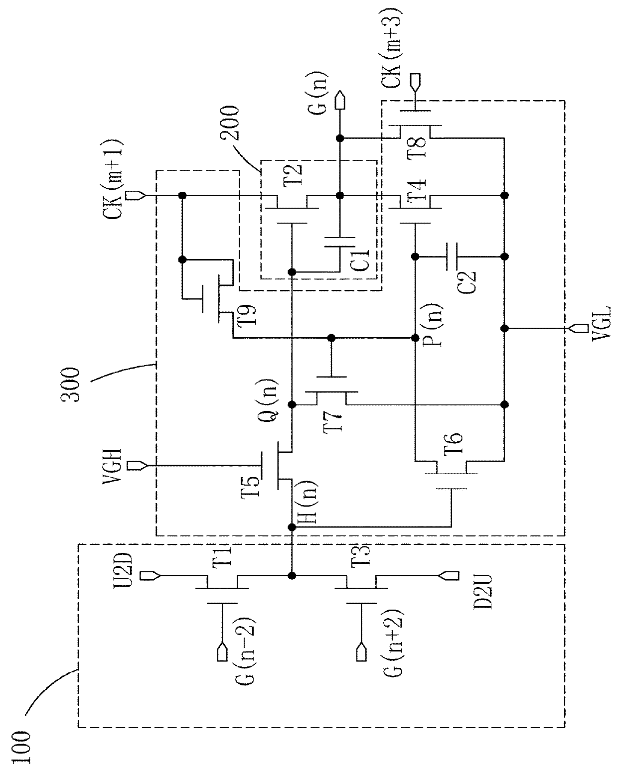
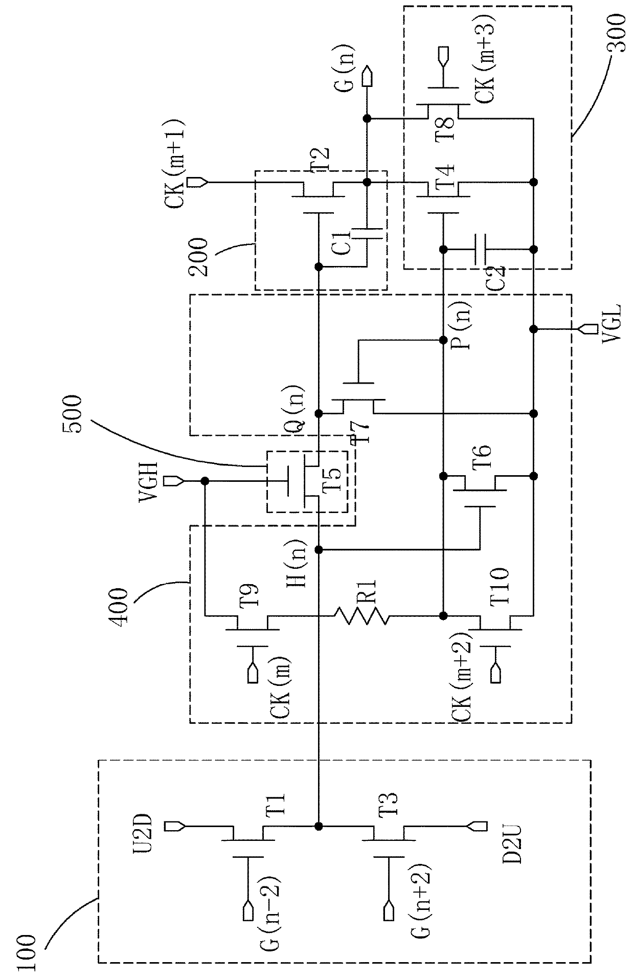
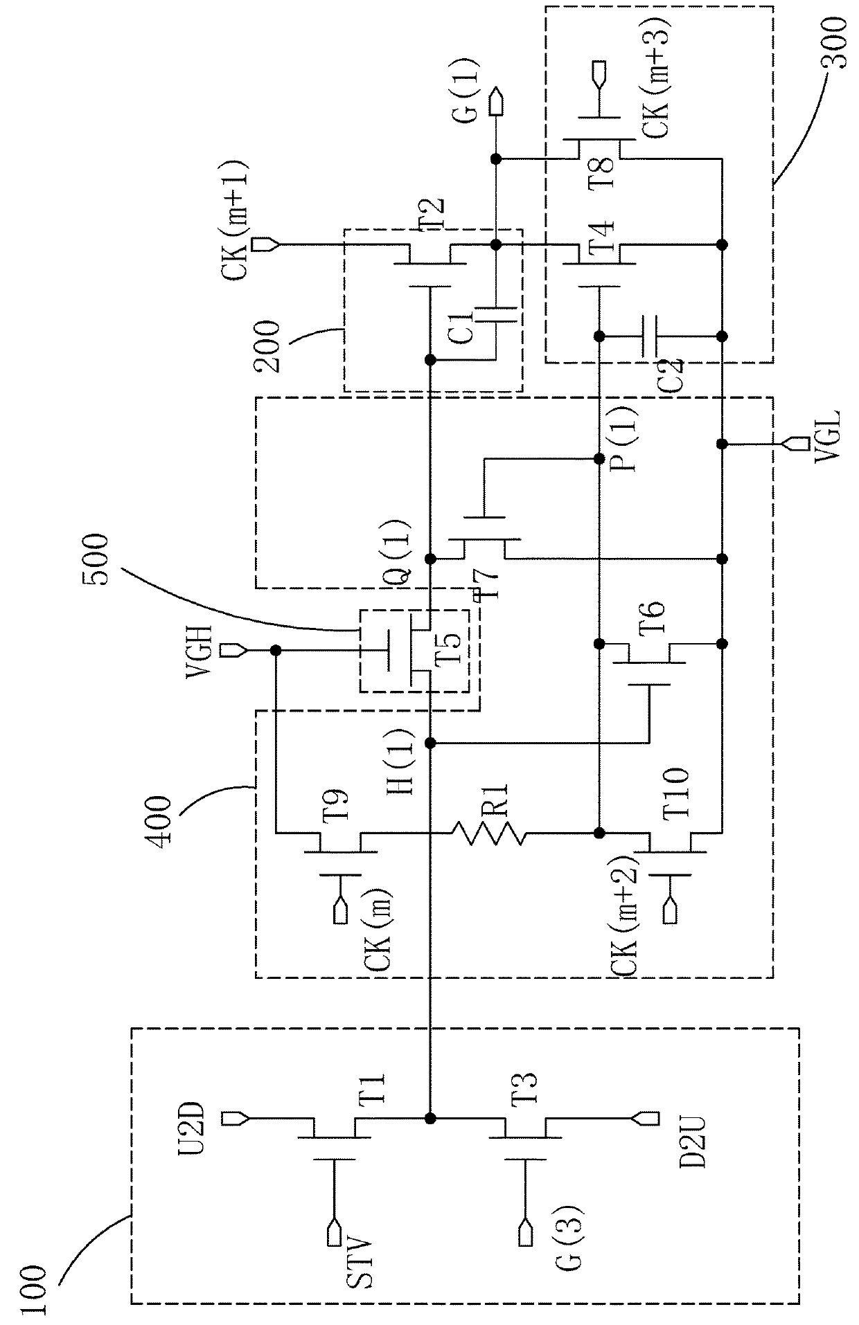
[0030]Refer to FIG. 2. The present invention provides a GOA circuit, which comprises: a plurality of cascade GOA units, each GOA unit comprising: a scan control module 100, an output module 200 connected to the scan control module 100, a pull-down module 300 connected to the output module 200, and a pull-down control module 400 connected to the scan control module 100, the output module 200 and the pull-down module 300.

[0031]For a positive integer n and a positive number m, other than the GOA unit in the first, the second, and the last two stages, in the n-th GOA unit, the scan control module 100 is for using a forward scan control signal U2D and a backward scan control signal D2U to control the GOA circuit to perform forward scanning or backward scanning.

[0032]The output module 200 is connected to an (m+1)-th clock signal CK(m+1...


PUM


Abstract

The invention provides a GOA circuit, using the ninth and tenth TFTs and the resistor to control the voltage level of the third node, wherein ninth TFT having the gate connected to the m-th clock signal, the source connected to the first constant voltage, and the drain connected to one end of the resistor; the tenth TFT having the gate connected to the (m+2)-th clock signal, the source connected to the second constant voltage, and the drain connected to the other end of the resistor. Through the m-th and the (m+2)-th clock signal to control the ninth and the tenth TFTs to become conductive alternately, the present invention can charge and discharge the third node regularly to prevent the threshold voltage shift of the key TFT because the third node stays high for extended time, and ensure the stability of GOA circuit.

Description

BACKGROUND OF THE INVENTION1. Field of the Invention[0001]The present invention relates to the field of display, and in particular to a gate driver on array (GOA) circuit.2. The Related Arts[0002]As the liquid crystal display (LCD) shows the advantages of being thin, low power-consumption, and no radiation, the LCD is widely used in various devices, such as, liquid crystal TV, mobile phones, PDA, digital camera, PC monitors or notebook PC screens as well as the leading technology in tablet PCs.[0003]The gate driver on array (GOA) technology is the array substrate column drive technology, by using the array substrate process for the LCD panel to manufacture the driver circuit for the horizontal scan line in the area around the active area on the substrate to replace the external integrated circuit (IC) to perform driving the horizontal scan lines. GOA technology can reduce the bonding process for the external IC and reduce cost, as well as the ability to realize narrow-border or bord...

Claims


Application Information

Patent Timeline
Patent Type & Authority Patents(United States)
IPC IPC(8): G09G3/36
CPCG09G3/3696G09G3/3648G09G3/3688G09G3/3677G09G2330/021G09G2310/08G09G2230/00G11C19/28G09G2300/0408G09G2310/0283G09G2310/0286G09G3/20
Inventor LI, YAFENG
Owner WUHAN CHINA STAR OPTOELECTRONICS TECH CO LTD
Why Eureka
Try Eureka