Replacement metal gate scheme with self-alignment gate for vertical field effect transistors

a vertical field effect transistor and self-aligning gate technology, applied in the direction of transistors, semiconductor devices, electrical equipment, etc., can solve the problems of reducing device reliability, vsub>t /sub>tolerance degradation, detrimental to analog circuits, etc., to maximize effective device width, improve device performance, and less defects during manufacturing

Active Publication Date: 2018-08-07
INT BUSINESS MASCH CORP
View PDF13 Cites 1 Cited by
  • Summary
  • Abstract
  • Description
  • Claims
  • Application Information

AI Technical Summary

Benefits of technology

[0016]The advantages of the present invention include forming the replaceable metal gate (RMG) after the formation of the top source / drain regions. Additional advantages include maximizing effective device width (i.e., number of fins) to improve device performance (i.e., by having more active fins). Moreover, lateral etching results in less defects during manufacturing and manufacturing costs can be reduced by, e.g., simplifying cell connectivity schemes.

Problems solved by technology

However, these metals alter their interface characteristics with the high-k dielectric after high-temperature processing which manifests itself as Vt variation and dielectric leakage.
These conditions lead to decreased device reliability.
This leads to difficulties in controlling Vt roll-off, that is, the rapid change in Vt with variation in gate length, thereby leading to Vt tolerance degradation, which is especially detrimental to analog circuits.
As a result, the performance of the VFET is affected.

Method used


Image

  • Replacement metal gate scheme with self-alignment gate for vertical field effect transistors
  • Replacement metal gate scheme with self-alignment gate for vertical field effect transistors
  • Replacement metal gate scheme with self-alignment gate for vertical field effect transistors

Examples


Embodiment Construction

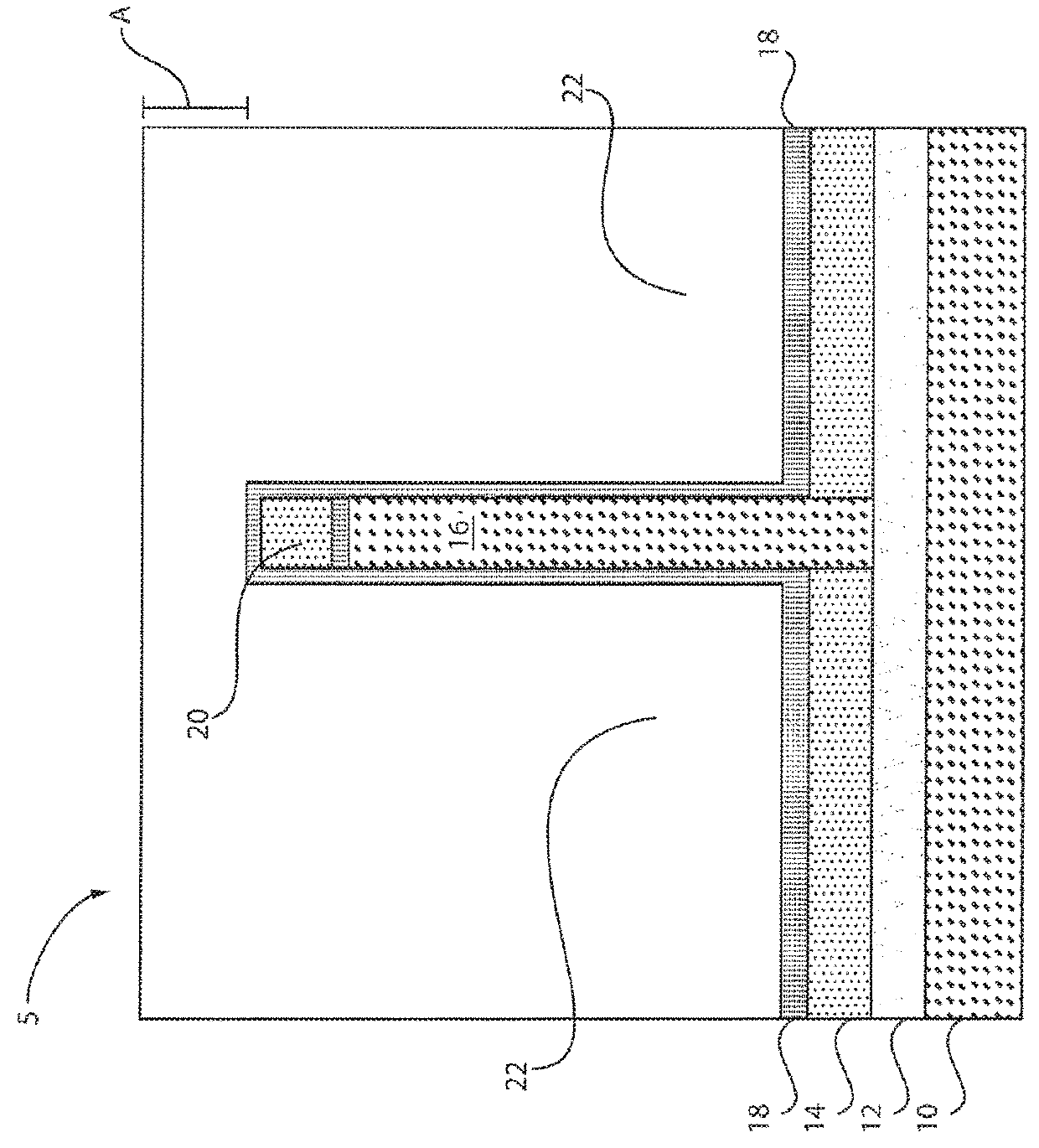
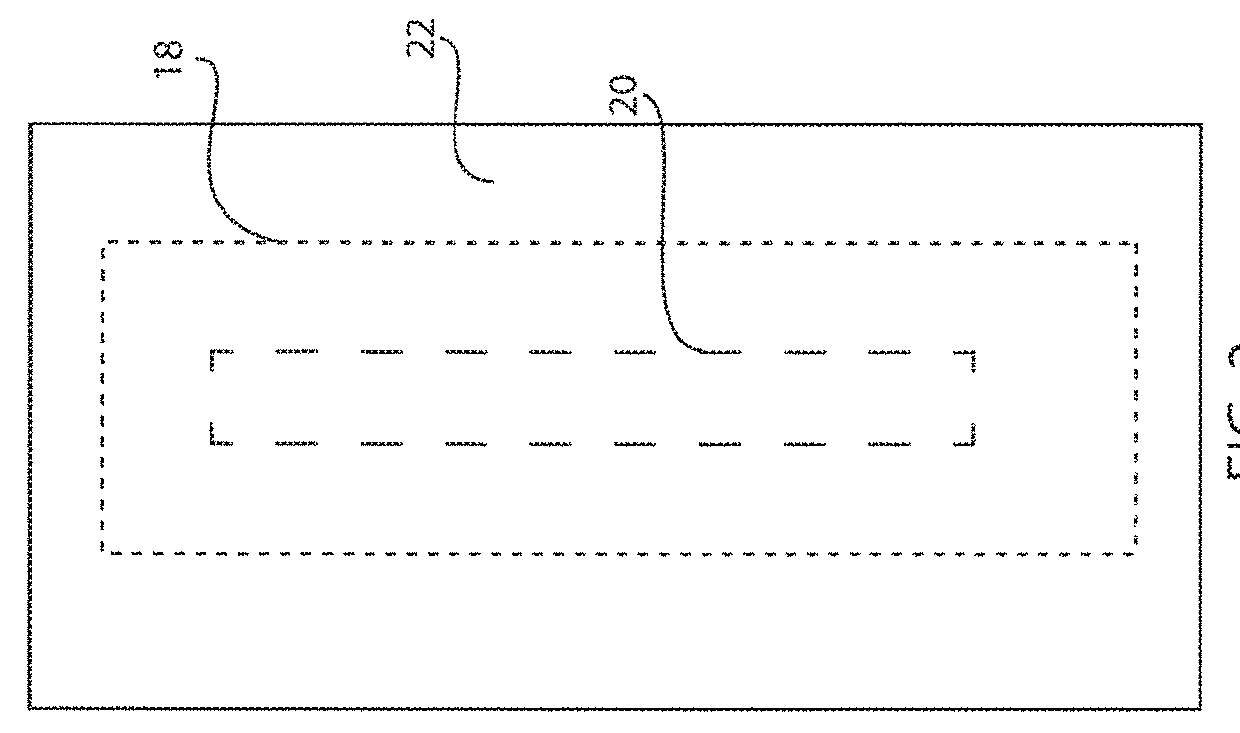
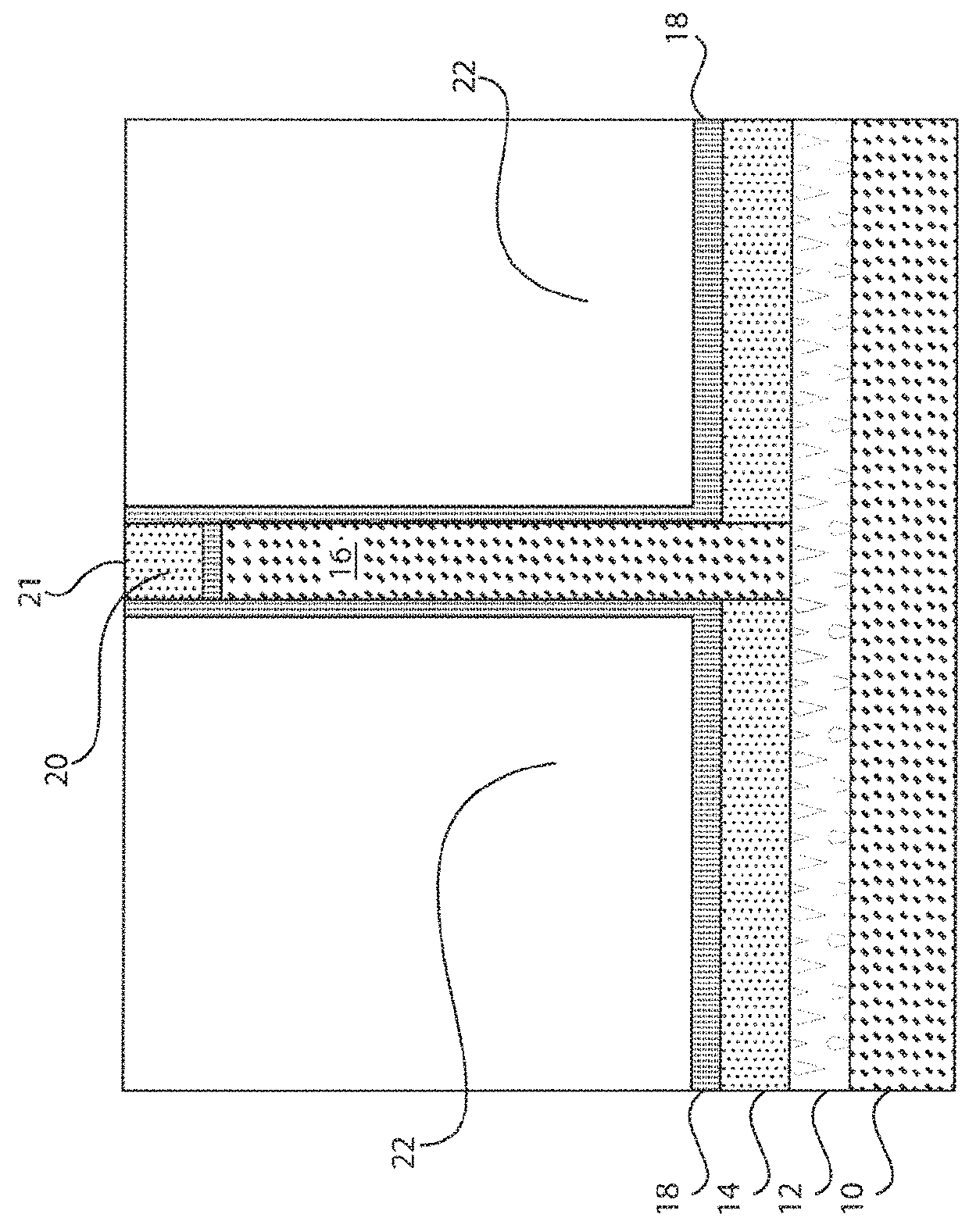
[0067]In one or more embodiments, a method advantageously includes forming a fin structure over a substrate, forming a dummy gate over the fin structure, and etching the dummy gate by a first amount to expose a top portion of the fin structure. The method further includes forming an oxide layer adjacent the exposed top portion of the fin structure, forming a spacer adjacent the oxide layer contacting the fin structure, and etching the dummy gate by a second amount. The method further includes depositing nitride to encapsulate the remaining dummy gate, depositing an inter-level dielectric (ILD) over the nitride, depositing at least one hard mask to access the dummy gate, stripping the dummy gate to form at least one recess, and filling the at least one recess with a high-k metal gate (HKMG).

[0068]In one or more embodiments, a semiconductor structure advantageously includes a fin structure formed over a substrate, a dummy gate formed over the fin structure, the dummy gate etched by a ...


PUM


Abstract

A method is presented for forming a semiconductor structure. The method includes forming a fin structure over a substrate, forming a dummy gate over the fin structure, and etching the dummy gate by a first amount to expose a top portion of the fin structure. The method further includes forming a first dielectric layer adjacent the exposed top portion of the fin structure, forming a spacer adjacent the first dielectric layer contacting the fin structure, and etching the dummy gate by a second amount. The method further includes depositing a second dielectric layer to encapsulate the remaining dummy gate, depositing an inter-level dielectric (ILD) over the second dielectric layer, depositing at least one hard mask to access the dummy gate, stripping the dummy gate to form at least one recess, and filling the at least one recess with a high-k metal gate (HKMG).

Description

BACKGROUNDTechnical Field[0001]The present invention relates generally to semiconductor devices, and more specifically, to a self-alignment gate for a vertical field effect transistor (VFET).Description of the Related Art[0002]A fin metal-oxide-semiconductor field effect transistor (finMOSFET or FinFET) can provide solutions to metal-oxide-semiconductor field effect transistor (MOSFET) scaling issues at and below, for example, the 22 nanometer (nm) node of semiconductor technology. A FinFET includes at least one narrow semiconductor fin (e.g., less than 30 nm wide) gated on at least two opposing sides of each of the at least one semiconductor fin. FinFET structures can, for example, typically be formed on either a semiconductor-on-insulator (SOI) substrate or a bulk semiconductor substrate.[0003]A feature of a FinFET is a gate electrode located on at least two sides of the channel formed along the longitudinal direction of the fin. Due to the feature of full depletion in the fin str...

Claims


Application Information

Patent Timeline
Patent Type & Authority Patents(United States)
IPC IPC(8): H01L21/8234H01L29/66H01L27/088H01L21/311H01L29/08H01L29/78H01L29/40H01L21/8238
CPCH01L29/6653H01L29/6656H01L21/31111H01L29/0847H01L29/7827H01L29/401H01L29/66545H01L29/66666H01L21/823431H01L21/823821H01L21/823468H01L27/0886
Inventor BAO, RAQIANGGUO, DECHAO
Owner INT BUSINESS MASCH CORP
Why Eureka
Try Eureka