
Motion sensor integrated nano-probe N/MEMS apparatus, method, and applications

a motion sensor and nano-probe technology, applied in the field of motion sensor integrated nano-electromechanical system apparatus, can solve the problems of parasitic capacitance, rf noise and charge coupling, previous efforts to integrate scanning system performance decline, etc., and achieve significant rf coupling noise, reduced noise, and increased impedance (1/jc).

Active Publication Date: 2018-08-14
CORNELL UNIVERSITY
View PDF10 Cites 11 Cited by
  • Summary
  • Abstract
  • Description
  • Claims
  • Application Information

AI Technical Summary

Benefits of technology

This patent describes a new device that allows for precise measurements of signals in a small and efficient way. This device uses a special type of semiconductor called JFETs, which are integrated into a micro-probe apparatus. The JFETs help to reduce interference from other components and create a local signal measurement system. They also provide a gain in signal strength and help to transform impedance, which reduces noise. Overall, this invention provides a better way to measure signals in a small and useful way.

Problems solved by technology

As capacitive transducers are scaled to nanoscale dimensions, their impedance (1 / jωC) is greatly increased, making them susceptible to parasitic capacitance, RF noise and charge coupling from local static and RF fields.
Previous efforts to integrate scanning systems have had lower performance due to noise coupling, as the wiring needed to connect to off-chip electronics added significant RF coupling noise.
First, the electrostatic force on the JFET induces a strain in the channel which tends to modify the channel carrier mobility of the JFET.

Method used


Image

  • Motion sensor integrated nano-probe N/MEMS apparatus, method, and applications
  • Motion sensor integrated nano-probe N/MEMS apparatus, method, and applications
  • Motion sensor integrated nano-probe N/MEMS apparatus, method, and applications

Examples


application examples

5. Application Examples

a. Resonance Frequency Measurement

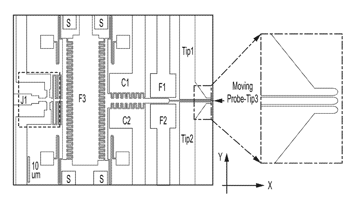
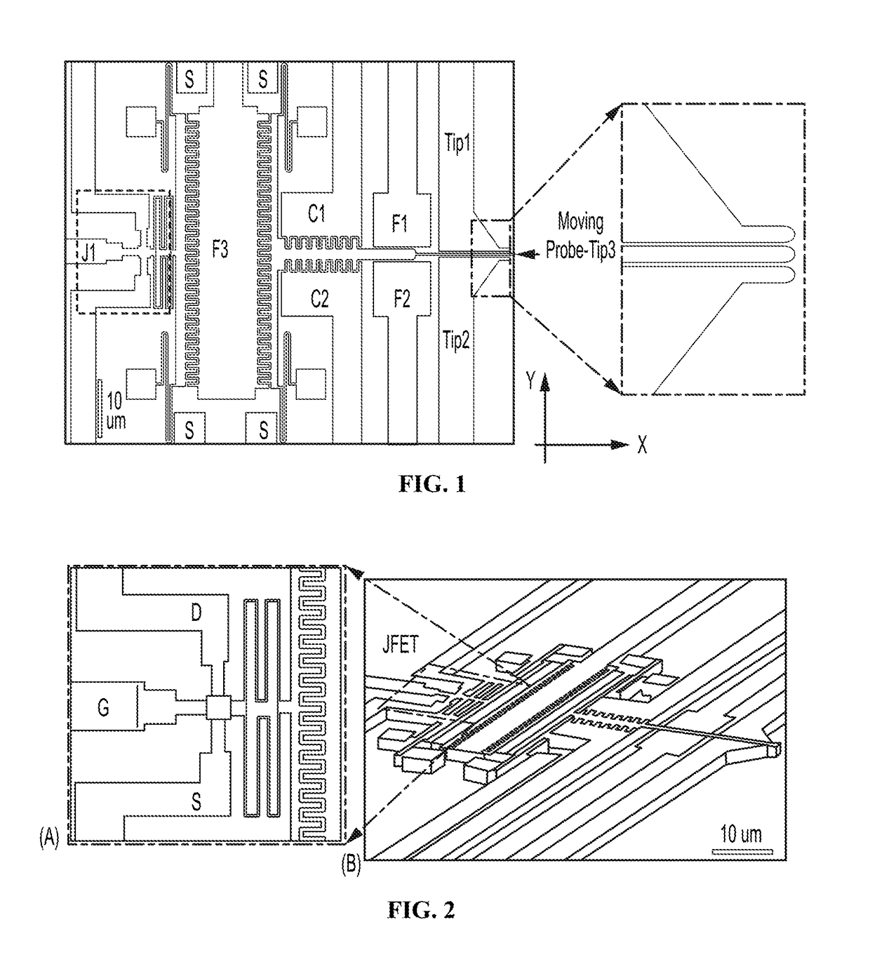
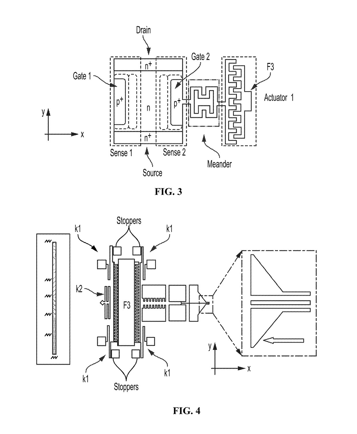
[0103]The multi-tip nano-probe apparatus that includes the JFET device in accordance with the embodiments may be employed in both AFM and STM applications. In these applications, the movable probe tip may be excited in resonance and scanned along a sample surface. Using an apparatus in accordance with the apparatus as illustrated in FIG. 16, the resonance frequency of a movable probe tip was measured in vacuum at 1.9 e-3 mbar.

[0104]The SOI substrate was grounded, and using a lock-In amplifier from Zurich Instruments (HF2LI), an AC sweep was combined with DC voltage through a bias-tee and launched on electrode F3. A displacement current through the movable probe tip was fed into an SR570 low noise transimpedance amplifier (TIA) with sensitivity set to 5 nA / V. The output of the TIA was fed into the lock-in amplifier for frequency domain analysis. FIG. 17 shows the measured fundamental resonance frequency of the movable probe tip...


PUM


Abstract

A multi-tip nano-probe apparatus and a method for probing a sample while using the multi-tip nano-probe apparatus each employ located over a substrate: (1) an immovable probe tip with respect to the substrate; (2) a movable probe tip with respect to the substrate; and (3) a motion sensor that is coupled with the movable probe tip. The multi-tip nano-probe apparatus and related method provide for improved sample probing due to close coupling of the motion sensor with the movable probe tip, and also retractability of the movable probe tip with respect to the immovable probe tip.

Description

CROSS-REFERENCE TO RELATED APPLICATION[0001]This application is related to, and derives priority from, U.S. Provisional Patent Application Ser. No. 61 / 576,455, filed 16 Dec. 2011 and titled Nano Probe Actuator, the content of which is incorporated herein fully by reference.STATEMENT OF GOVERNMENT INTEREST[0002]The research that lead to the embodiments as described herein, and the invention as claimed herein, was funded by the United States National Science Foundation under cooperative agreement DMR 1120296. The United States Government has rights in the invention as claimed herein.BACKGROUND[0003]Field of the Invention[0004]Embodiments relate generally to nano-scale microelectromechanical system (N / MEMS) apparatus and related methods. More particularly, embodiments relate to motion actuation and sensor integrated nano-scale microelectromechanical system apparatus and related methods.[0005]Description of the Related Art[0006]Nano-probe tip-based nano-fabrication processes often requi...

Claims


Application Information

Patent Timeline
Patent Type & Authority Patents(United States)
IPC IPC(8): G01Q70/08G01Q20/00G01Q10/00G01Q70/06G01Q60/30
CPCG01Q20/00G01Q10/00G01Q70/08G01Q70/06G01Q60/30
Inventor LAL, AMITAMPONSAH, KWAME
Owner CORNELL UNIVERSITY
Learn More