QFN pre-molded leadframe having a solder wettable sidewall on each lead

a pre-molded, leadframe technology, applied in the direction of semiconductor devices, semiconductor/solid-state device details, electrical apparatus, etc., can solve the problems of less resistance and lower thermal load per solder pin, and achieve the effect of reducing the likelihood of leadframe damag

Active Publication Date: 2018-09-18
STMICROELECTRONICS INT NV
View PDF4 Cites 21 Cited by
  • Summary
  • Abstract
  • Description
  • Claims
  • Application Information

AI Technical Summary

Benefits of technology

[0007]With the molds in place, molding compound is formed in the apertures between the die pads of the leadframe and in the cavities of the top mold tool. When the top and bottom mold tools are released, a pre-molded leadframe remains with molding compound in the plurality of apertures and on a first surface of the leadframe. The molding compound in the pre-molded leadframe provides additional support to the leadframe above the plurality of recesses, which prevents leadframe bouncing during processing and thereby reduces the likelihood of leadframe damage during incorporation of the leadframe into a package. Once the pre-molded leadframe is formed, the leadframe is incorporated into a package by coupling one or more die to each die pad and coupling a plurality of wires between each die and the metal layer on one or more leads. Then, an encapsulant is formed over the die, the wires and the pre-molded leadframe. The resulting combination is then separated with a mechanical blade or other cutting means at the plurality of recesses to form packages with solder wettable sidewalls.

Problems solved by technology

This also increases the solder contact area between the package and the PCB, which results in less resistance and a lower thermal load per solder pin.

Method used


Image

  • QFN pre-molded leadframe having a solder wettable sidewall on each lead
  • QFN pre-molded leadframe having a solder wettable sidewall on each lead
  • QFN pre-molded leadframe having a solder wettable sidewall on each lead

Examples


Embodiment Construction

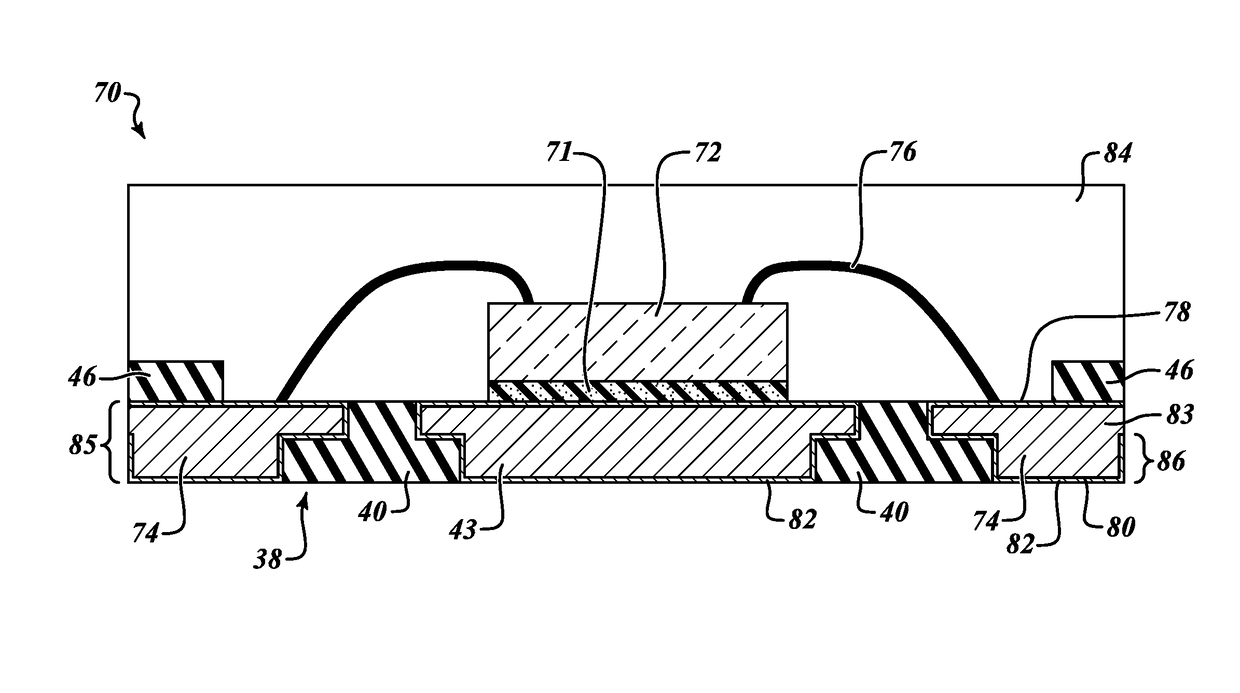
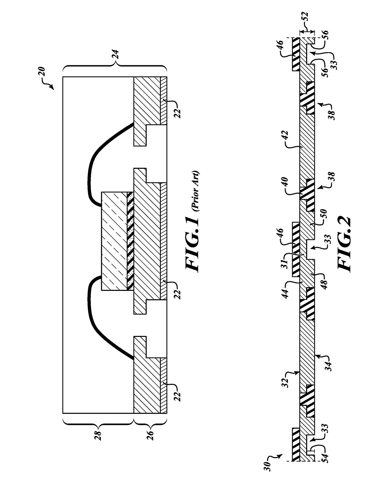
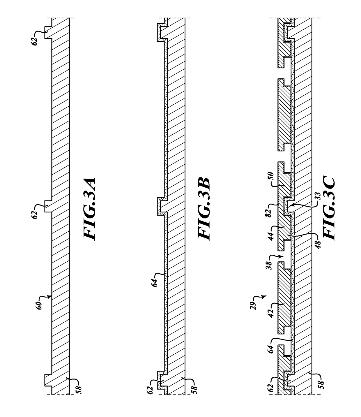
[0016]In the following description, certain specific details are set forth in order to provide a thorough understanding of various embodiments of the disclosure. However, one skilled in the art will understand that the disclosure may be practiced without these specific details. In other instances, well-known structures associated with electronic components and fabrication techniques have not been described in detail to avoid unnecessarily obscuring the descriptions of the embodiments of the present disclosure. The drawings are not necessarily drawn to scale and some features are enlarged to provide a more clear view of particular features.

[0017]Unless the context requires otherwise, throughout the specification and claims that follow, the word “comprise” and variations thereof, such as “comprises” and “comprising,” are to be construed in an open, inclusive sense, that is, as “including, but not limited to.”

[0018]The use of ordinals such as first, second and third does not necessaril...


PUM


Abstract

The present disclosure is directed to a leadframe package having solder wettable sidewalls that is formed using a pre-molded leadframe and methods of manufacturing the same. A metal plated leadframe with a plurality of recesses and a plurality of apertures is placed into a top and bottom mold tool. A molding compound is then formed in the plurality of recesses and apertures in the leadframe to form a pre-molded leadframe. A plurality of die and wires are coupled to the pre-molded leadframe and the resulting combination is covered in an encapsulant. Alternatively, a bare leadframe can be processed and the metal layer can be applied after encapsulation. A saw or other cutting means is used for singulation to form leadframe packages. Each resulting leadframe package has a solder wettable sidewall for improving the strength of solder joints between the package and a circuit board.

Description

BACKGROUNDTechnical Field[0001]The present disclosure is directed to a leadframe package with a solder wettable sidewall formed using a pre-molded leadframe and methods of manufacturing the same.Description of the Related Art[0002]A typical semiconductor package includes a die coupled to a leadframe and various electrical contacts. The resulting combination is then covered with an encapsulant to create the package. Lands (also referred to as leads) located on a bottom surface of the package and, in many cases, side surfaces of the package provide electrical connection to a circuit board, such as a printed circuit board (PCB). When coupling the package to the PCB, the packages are mounted directly on the surface of the PCB using surface mount technology (SMT).[0003]Although SMT allows for smaller packages, it also creates some disadvantages. In particular, the solder joints between the package and the PCB can be weakened due to the PCB and the package having different coefficients of...

Claims


Application Information

Patent Timeline
Patent Type & Authority Patents(United States)
IPC IPC(8): H01L23/495H01L21/56H01L21/78H01L23/31H01L21/48
CPCH01L23/49541H01L23/4952H01L21/78H01L23/49503H01L23/3192H01L21/565H01L21/4853H01L23/49582H01L23/495H01L24/42H01L23/49548H01L23/3121H01L21/561H01L2224/48091H01L2224/97H01L2924/181H01L2224/48247H01L2224/73265H01L2924/00014H01L2924/00012H01L23/49861
Inventor CADAG, AARONANTILANO, JR., ERNESTOCADAG, ELA MIA
Owner STMICROELECTRONICS INT NV
Why Eureka
Try Eureka