Reverse-conducting semiconductor device

a reverse-conducting, semiconductor technology, applied in semiconductor devices, diodes, electrical devices, etc., can solve the problem of affecting the soa of the freewheeling diodes, and achieve the effect of improving the turn-off capability of the device in diode mod

Active Publication Date: 2018-10-23
HITACHI ENERGY LTD
View PDF12 Cites 4 Cited by
  • Summary
  • Abstract
  • Description
  • Claims
  • Application Information

AI Technical Summary

Benefits of technology

[0026]It is an object of the invention to provide a reverse-conducting MOS device having an improved turn-off capability of the device in diode mode.
[0032]Due to the additional p-bars high turn-off capability of the IGBT can be obtained and snap-back free characteristics in the diode mode can be enabled.
[0033]The VLD layer is used for reducing the electric field in the termination region. As the VLD layer is connected to the bar and as the protection layer is embedded in the VLD layer, the electric field is reduced in a small distance, i.e. the need to have a wide field ring structure.
[0034]Due to the introduction of the highly doped protection layer the holes are directed not into a small spot area at the interface between the bar and the variable-lateral doping-layer, but they are spread more widely within the protection layer and an additional resistance is introduced into the filament path which reduces the filament current. This effect can further be enhanced by having a protection layer with a plurality of protection regions, exemplarily by having ring-shaped regions (protection rings) surrounding the active cell region, each of which encloses the active cell region and which separated from each other by the lower doped VLD layer. The protection regions, which are farer away from the bar region, enclose the protection regions, which are nearer to the bar region, in a plane parallel to the first main side. By the protection regions being embedded in the VLD layer, in planes parallel to the first main side, a modulated doping profile (of the second conductivity type) is achieved, in which at the protection regions a higher doping concentration is present than at the VLD layer in-between such protection regions. In an exemplary embodiment, the device has up to 5 protection rings or between 3 and 5 protection rings as protection regions.
[0035]This effect results in a drastic reduction of the maximum temperature in the termination region, i.e. in the filament as shown in FIG. 4. Inventive RC-IGBT1 contains five protection regions with decreasing widths and Inventive RC-IGBT2 contains two protection regions with constant widths. At the same voltage and current as for the prior art device, the hole current is spread out and does not focus into a narrow filament. As a result, peak temperature in the device is reduced which in turn provides much better turn-off capability of the diode and much better SOA performance in diode mode is achievable.
[0036]The invention combines the advantage of keeping the temperature low in the device with a small termination width (i.e. having a small width in a direction of increasing distance from the active cell region).

Problems solved by technology

However, the SOA of the freewheeling diode is affected strongly by the design of the p-bars contact with the termination region in the areas around the active area of the BIGT / RC-IGBT.

Method used


Image

  • Reverse-conducting semiconductor device
  • Reverse-conducting semiconductor device
  • Reverse-conducting semiconductor device

Examples


Embodiment Construction

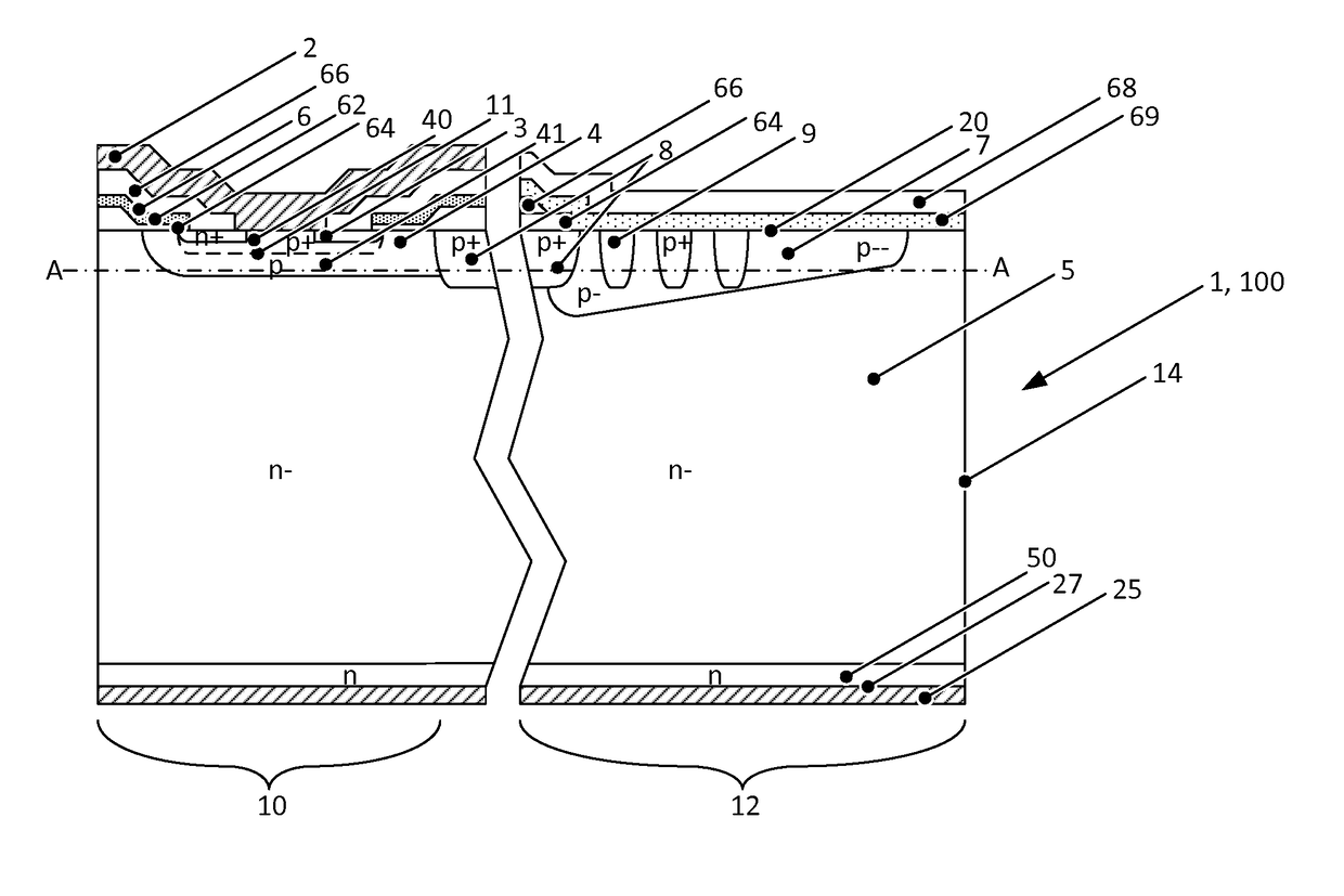
[0055]In FIG. 5 a first embodiment of an inventive reverse-conducting (RC) MOS (metal oxide semiconductor) device 1 in form of a metal-oxide-semiconductor field-effect transistor (MOSFET) 100 is shown. The MOSFET 100 comprises a first main electrode 2, which is a source electrode for a MOSFET, on a first main side 20 and a second main electrode 25, which is a drain electrode for the MOSFET 100, on a second main side 27 opposite to the first main side 20. The device has an active cell region 10 (central region, which shall be a MOS cell region, i.e. such region, in which the MOS cells 11 are arranged) and a termination region 12 laterally surrounding the active cell region 10 up to an edge 14 of the device. The edge is arranged as the surface of the device between the first and second main side 20, 27 of the device. The first main side 20 shall be the surface of the doped layers on the side towards the first main electrode 2. It shall be a plain plane farthest away from the second ma...


PUM


Abstract

A reverse-conducting MOS device is provided having an active cell region and a termination region. Between a first and second main side. The active cell region comprises a plurality of MOS cells with a base layer of a second conductivity type. On the first main side a bar of the second conductivity type, which has a higher maximum doping concentration than the base layer, is arranged between the active cell region and the termination region, wherein the bar is electrically connected to the first main electrode. On the first main side in the termination region a variable-lateral-doping layer of the second conductivity type is arranged. A protection layer of the second conductivity type is arranged in the variable-lateral-doping layer, which protection layer has a higher maximum doping concentration than the maximum doping concentration of the variable-lateral-doping layer in a region attached to the protection layer.

Description

TECHNICAL FIELD[0001]The invention relates to the field of power electronics and more particularly to a reverse-conducting MOS device according to the preamble of claim 1.BACKGROUND ART[0002]In U.S. Pat. No. 8,212,283 B2 a prior art reverse-conducting insulated gate bipolar transistor (RC-IGBT) in form of a Bi-mode Insulated Gate Transistor (BIGT) 160 is described (shown in FIG. 1), which comprises a freewheeling diode and an insulated gate bipolar transistor (IGBT) on a common semiconductor chip, part of which chip forms the (n−) doped drift layer 5 with a drift layer doping concentration and a drift layer thickness 53. The RC-IGBT comprises an anode side 27 (second main side) and a cathode side 20 (first main side), whereas the anode side 27 is arranged opposite of the cathode side 20 of the chip.[0003]The drift layer thickness 53 is the maximum vertical distance between the anode and cathode side 27 and 20 of that part of the chip with the drift layer doping concentration.[0004]A...

Claims


Application Information

Patent Timeline
Patent Type & Authority Patents(United States)
IPC IPC(8): H01L29/66H01L29/739H01L29/40H01L29/36H01L29/78H01L29/06H01L29/10H01L29/08
CPCH01L29/7395H01L29/0615H01L29/0619H01L29/0692H01L29/0696H01L29/0865H01L29/1004H01L29/1095H01L29/36H01L29/402H01L29/7811H01L29/7819H01L29/7823H01L29/063H01L29/0834H01L29/7396
Inventor STORASTA, LIUTAURASCORVASCE, CHIARALE GALLO, MANUELRAHIMO, MUNAFKOPTA, ARNOST
Owner HITACHI ENERGY LTD
Why Eureka
Try Eureka