Thinned electronic product and manufacturing method thereof
a technology of electronic products and manufacturing methods, applied in the direction of decalcomania, conductive pattern formation, association of printed circuit non-printed electric components, etc., can solve the problems of high yield loss, and achieve the effect of saving material costs and simplifying the manufacturing process of electronic products
- Summary
- Abstract
- Description
- Claims
- Application Information
AI Technical Summary
Benefits of technology
Problems solved by technology
Method used
Image
Examples
first embodiment
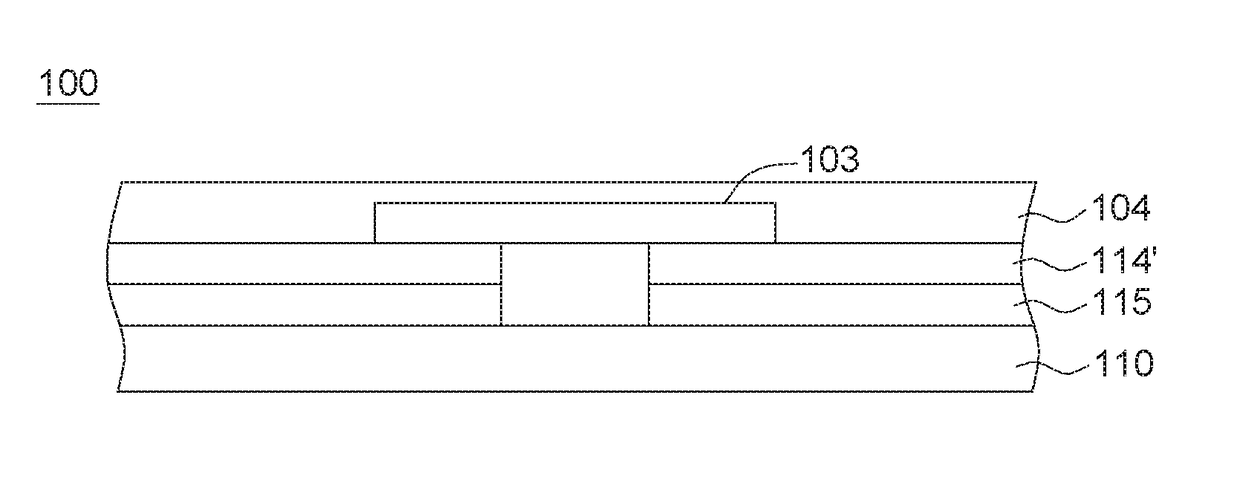
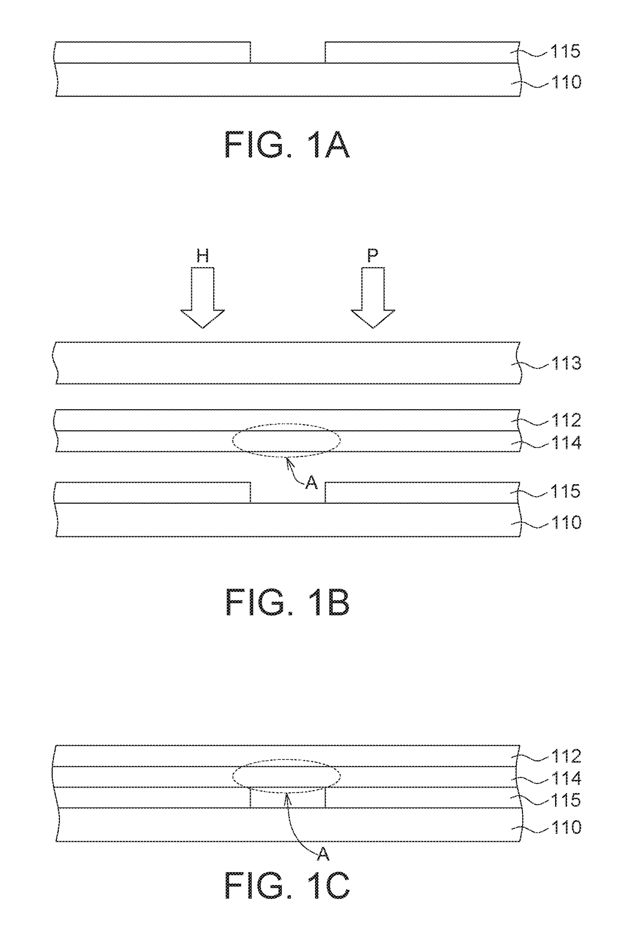
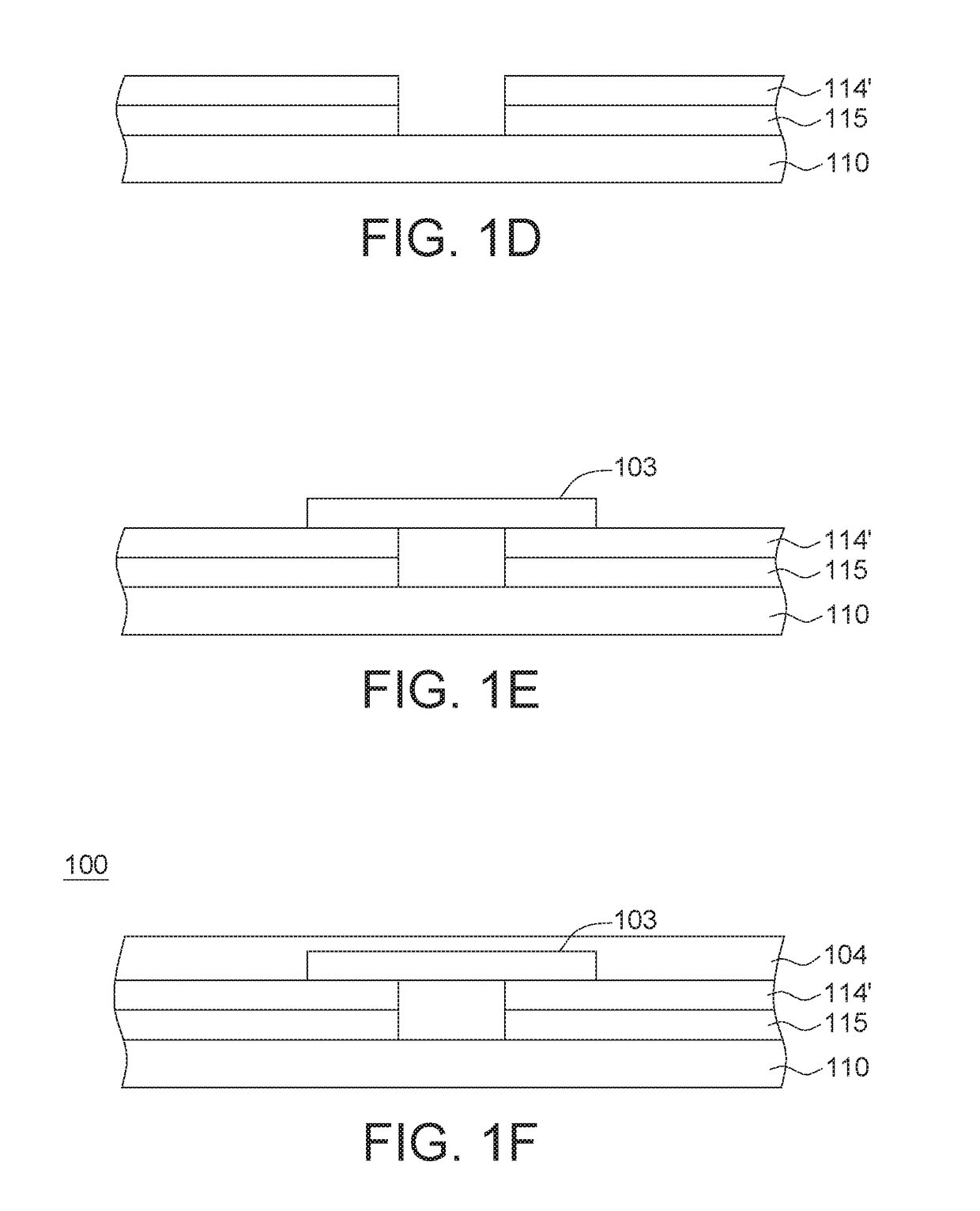
[0021]Refer to FIGS. 1A-1F. The manufacturing method of a thinned electronic product 100 in which a conductive circuit 114′ is formed by a hot stamping process according to the present invention is includes following steps. Firstly, as indicated in FIG. 1A, a patterned hot melt ink layer 115 is formed on a supporting body 110 by a printing process using a laser printer. The patterned hot melt ink layer 115 can be formed of a toner having an organic binder, and the toner may include 20-30% of ceramic powder (such as F—Fe3O4 crystal powder), 50-60% of polymer resin, 10-20% of charge modifier, fluidizer or surface modifier. The patterned hot melt ink layer 115 has a circuit pattern. After the patterned hot melt ink layer 115 is heated, an adhesion effect will be generated for bonding the patterned hot melt ink layer 115 on the conductive circuit 114′ in a hot pressing process. In an embodiment, the supporting body 110 can be formed of any non-conductive organic or inorganic materials s...
second embodiment
[0032]Refer to FIGS. 2A-2F. A manufacturing method of a thinned electronic product 100 in which a conductive circuit 114′ is formed by a hot stamping process according to the invention includes following steps. Firstly, as indicated in FIG. 2A, a conductive metal layer 114a having a releasing layer 112, preferably a heat resistant releasing layer, is formed on a toppan stamping plate 113a, and the heat resistant releasing layer 112 can be selectively disposed on the conductive metal layer 114a, that is, the conductive metal layer 114a having the heat resistant releasing layer 112 or without the heat resistant releasing layer 112, is placed on the toppan stamping plate 113a. As indicated in FIG. 2A, the heat resistant releasing layer 112 is close to the protrusion R of the toppan stamping plate 113a, the protrusion R has a circuit pattern, and the conductive metal layer 114a has a binder providing adhesion to the conductive metal layer 114a.
[0033]As indicated in FIG. 2B, a supportin...
fourth embodiment
[0037]Refer to FIGS. 4A-4F. The manufacturing method of a thinned electronic product 100 in which a conductive circuit 117′ is formed by a cold stamping process according to the invention includes following steps. Firstly, as indicated in FIG. 4A, a binder (such as UV curing adhesive) is formed on the supporting body 110 in a printing or a bonding manner to form a patterned binder layer 116 having a circuit pattern. As indicated in FIG. 4B, the conductive metal layer 117 having a resistant releasing layer 112′, preferably a light resistant releasing layer, is disposed on the patterned binder layer 116, and the light resistant releasing layer 112′ can be selectively disposed on the conductive metal layer 117, that is, the conductive metal layer 117 having the light resistant releasing layer 112′ or without the light resistant releasing layer 112′ can be placed on the patterned binder layer 116. Then, a pressure P is applied to the conductive metal layer 117 through the pressure plate...
PUM
 Abstract
Description
Claims
Application Information


