Semiconductor device

a semiconductor and semiconductor technology, applied in the field of semiconductor devices, can solve the problems of low power consumption of the display device in which a transistor including an oxide semiconductor is used, and achieve the effects of low leakage current, high on-state current, and stable electrical characteristics

Active Publication Date: 2018-12-04
SEMICON ENERGY LAB CO LTD
View PDF158 Cites 2 Cited by
  • Summary
  • Abstract
  • Description
  • Claims
  • Application Information

AI Technical Summary

Benefits of technology

[0010]An object is to provide a transistor with stable electrical characteristics. Another object is to provide a transistor having a low leakage current in an off state. Another object is to provide a transistor having a high on-state current. Another object is to provide a transistor with normally-off electrical characteristics. Another object is to provide a transistor with a small subthreshold swing value. Another object is to provide a highly reliable transistor.
[0026]A transistor with stable electrical characteristics can be provided. A transistor having a low leakage current in an off state can be provided. A transistor having a high on-state current can be provided. A transistor with normally-off electrical characteristics can be provided. A transistor with a small subthreshold swing value can be provided. A highly reliable transistor can be provided.

Problems solved by technology

For example, a display device in which a transistor including an oxide semiconductor is used is known to have low power consumption.

Method used


Image

  • Semiconductor device
  • Semiconductor device
  • Semiconductor device

Examples


embodiment 1

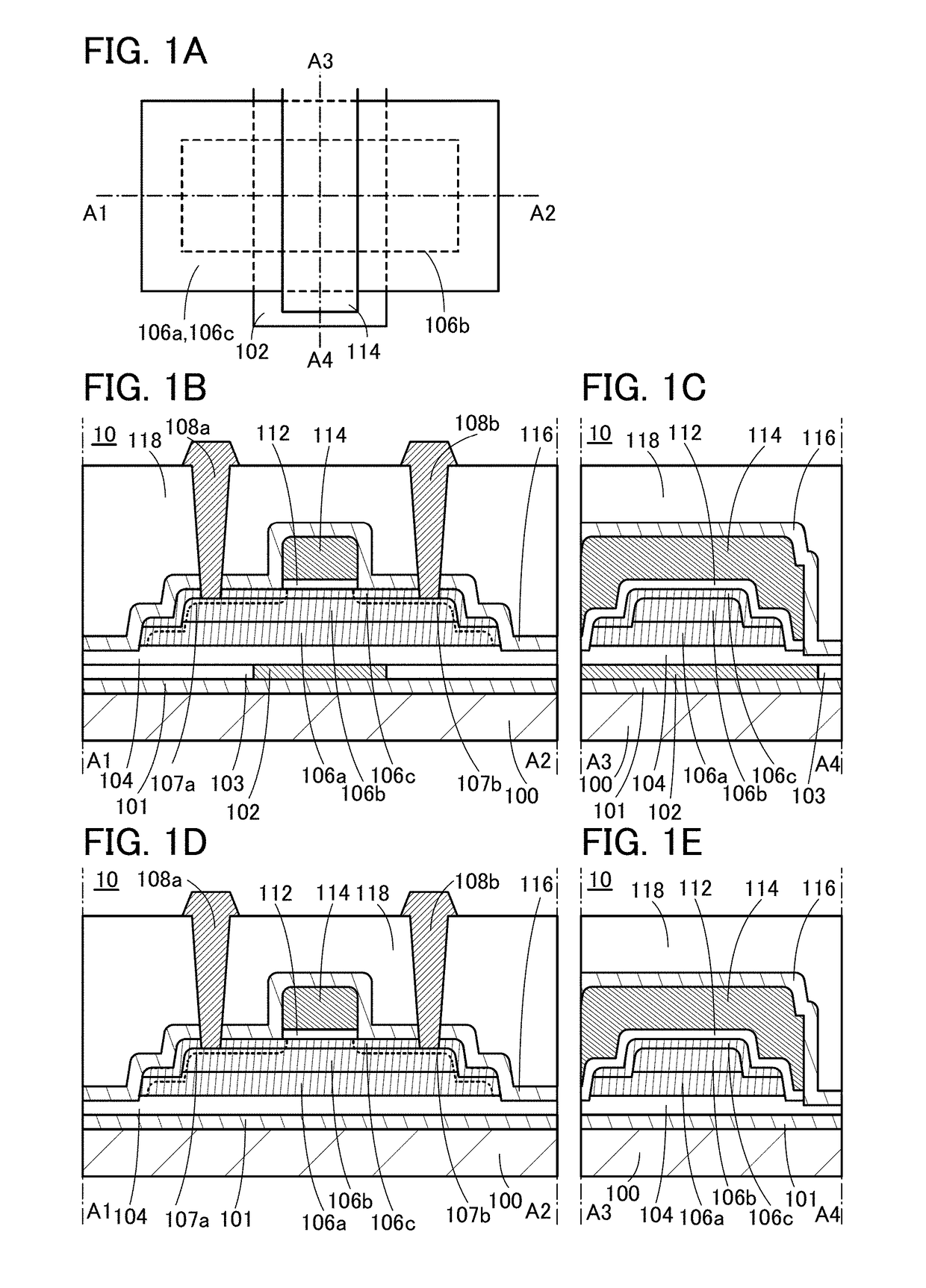
[0088]In this embodiment, structures of semiconductor devices of embodiments of the present invention will be described with reference to FIGS. 1A to 1E, FIGS. 2A to 2D, and FIGS. 3A to 3C.

[0089]Structures of transistors, which are examples of the semiconductor devices of embodiments of the present invention, will be described below.

[0090]A structure of a transistor 10 will be described with reference to FIGS. 1A to 1C. FIG. 1A is a top view of the transistor 10. FIG. 1B is a cross-sectional view taken along dashed-dotted line A1-A2 in FIG. 1A. FIG. 1C is a cross-sectional view taken along dashed-dotted line A3-A4 in FIG. 1A. A region along dashed-dotted line A1-A2 shows a structure of the transistor 10 in the channel length direction, and a region along dashed-dotted line A3-A4 shows a structure of the transistor 10 in the channel width direction. The channel length direction of a transistor refers to a direction in which carriers move between a source (source region or source elec...

modification example 1

of Transistor

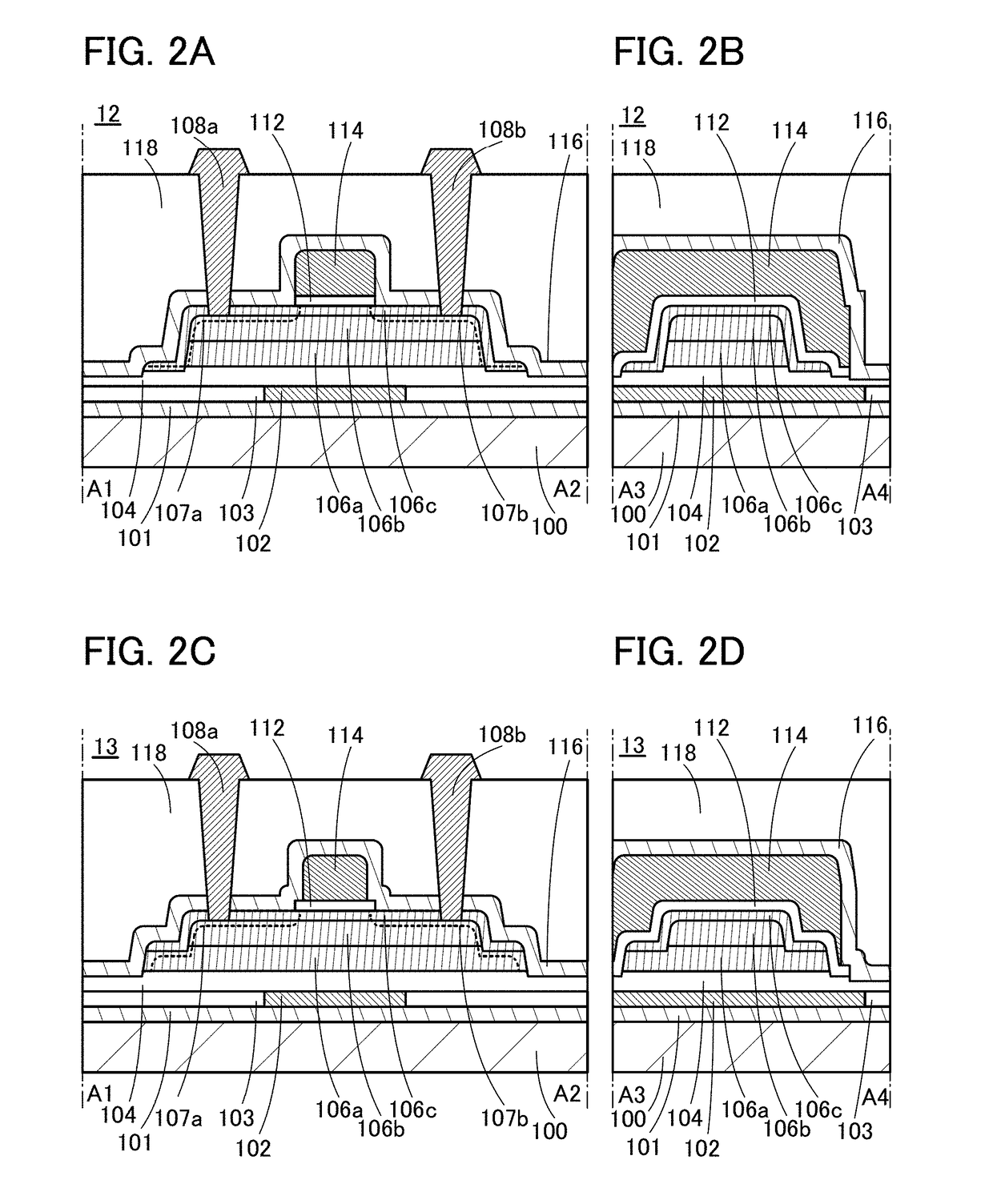
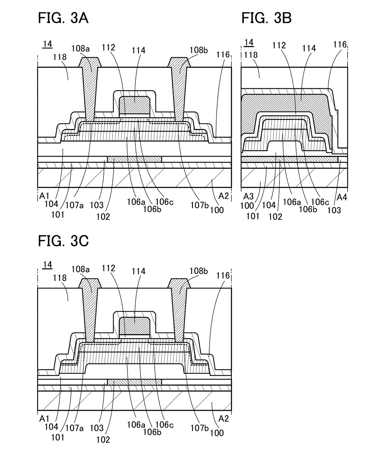
[0186]Modification examples of the transistor 10 are described below with reference to FIGS. 2A to 2D and FIGS. 3A to 3C. FIGS. 2A to 2D and FIGS. 3A to 3C are cross-sectional views of the transistors in the channel length direction and those in the channel width direction like FIGS. 1B and 1C. Note that the components in the following modification examples of the transistor 10 can be combined with each other as appropriate.

[0187]A transistor 12 illustrated in FIGS. 2A and 2B is different from the transistor 10 in that the end portion of the side surface of the insulator 106a is substantially aligned with the end portion of the side surface of the semiconductor 106b. Here, the thickness of the insulator 106a is preferably larger than the sum of the thicknesses of the insulator 106c and the insulator 112. With such a structure, substantially the entire side surface of the semiconductor 106b in the channel width direction can face the conductor 114 with the insulator 106c...

embodiment 2

[0196]In this embodiment, a method for manufacturing the semiconductor device of one embodiment of the present invention will be described with reference to FIGS. 4A to 4F and FIGS. 5A to 5D.

[0197]A method for manufacturing the transistor 10 illustrated in FIGS. 1A to 1E will be described below.

[0198]First, the substrate 100 is prepared. Any of the above-mentioned substrates can be used for the substrate 100.

[0199]Next, the insulator 101 is formed. Any of the above-mentioned insulators can be used for the insulator 101.

[0200]The insulator 101 can be formed by a sputtering method, a chemical vapor deposition (CVD) method, a molecular beam epitaxy (MBE) method, a pulsed laser deposition (PLD) method, an atomic layer deposition (ALD) method, or the like.

[0201]CVD methods can be classified into a plasma enhanced CVD (PECVD) method using plasma, a thermal CVD (TCVD) method using heat, a photo CVD method using light, and the like. Moreover, the CVD method can include a metal CVD (MCVD) me...


PUM


Abstract

A transistor with stable electrical characteristics. A semiconductor device that includes an oxide semiconductor, a first conductor, a first insulator, a second insulator, a third insulator, and a fourth insulator. The oxide semiconductor is positioned over the first insulator. The second insulator is positioned over the oxide semiconductor. The third insulator is positioned over the second insulator. The first conductor is positioned over the third insulator. The fourth insulator is positioned over the first conductor. The fourth insulator includes a region in contact with a top surface of the second insulator. The oxide semiconductor includes a region overlapping with the first conductor with the second insulator and the third insulator positioned therebetween. When seen from above, a periphery of the first insulator and a periphery of the second insulator are located outside a periphery of the oxide semiconductor.

Description

BACKGROUND OF THE INVENTION[0001]1. Field of the Invention[0002]The present invention relates to, for example, a transistor or a semiconductor device. The present invention relates to, for example, a method for manufacturing a transistor or a semiconductor device. The present invention relates to, for example, a display device, a light-emitting device, a lighting device, a power storage device, a memory device, a processor, or an electronic device. The present invention relates to a method for manufacturing a display device, a liquid crystal display device, a light-emitting device, a memory device, or an electronic device. The present invention relates to a driving method of a display device, a liquid crystal display device, a light-emitting device, a memory device, or an electronic device.[0003]Note that one embodiment of the present invention is not limited to the above technical field. The technical field of one embodiment of the invention disclosed in this specification and the ...

Claims


Application Information

Patent Timeline
Patent Type & Authority Patents(United States)
IPC IPC(8): H01L29/78H01L29/786H01L29/24H01L29/51H01L29/49
CPCH01L29/7869H01L29/24H01L29/4908H01L29/78696H01L29/517H01L29/78603H01L29/78648H01L29/513H01L27/1207H01L27/1225H01L27/1248
Inventor YAMAZAKI, SHUNPEI
Owner SEMICON ENERGY LAB CO LTD
Why Eureka
Try Eureka