Semiconductor stack for converter with snubber capacitors

a technology of snubber capacitors and semiconductors, which is applied in the direction of semiconductor devices, solid-state devices, basic electric elements, etc., can solve the problems of reducing the performance or switching speed of two-level converters, voltage spikes that load semiconductor switches,

Active Publication Date: 2018-12-25
HITACHI ENERGY LTD
View PDF27 Cites 0 Cited by
  • Summary
  • Abstract
  • Description
  • Claims
  • Application Information

AI Technical Summary

Benefits of technology

[0007]It is an object of the invention to provide a semiconductor stack for a converter which is constructed compactly and which has a low leakage inductance in the commutation loop.
[0011]A structurally compact semiconductor stack having a low leakage inductance in the commutation loops can be provided in this way. Since parallel-connected inductances lead to a lower inductance, a plurality of commutation loops, (two, three, four, etc.) lead to a reduction of the leakage inductance. Since a plurality of small capacitors, rather than one large capacitor, can be distributed around the semiconductor stacks, the structural space can additionally be better utilized.
[0014]In accordance with one embodiment of the invention, the semiconductor stack further comprises a snubber diode. The parallel-connected snubber capacitors can be connected to one end of the two series-connected semiconductor switches via a diode, which can prevent oscillations or resonances in the commutation loops.

Problems solved by technology

If a commutation of the current occurs between the two switches, the current does not fall abruptly owing to the leakage inductance, but rather is temporally dependent, which leads to voltage spikes that load the semiconductor switches.
Since each semiconductor switch can also block only a limited voltage at its inputs, a high leakage inductance also reduces the performance or switching speed of the two-level converter.

Method used


Image

  • Semiconductor stack for converter with snubber capacitors
  • Semiconductor stack for converter with snubber capacitors
  • Semiconductor stack for converter with snubber capacitors

Examples


Embodiment Construction

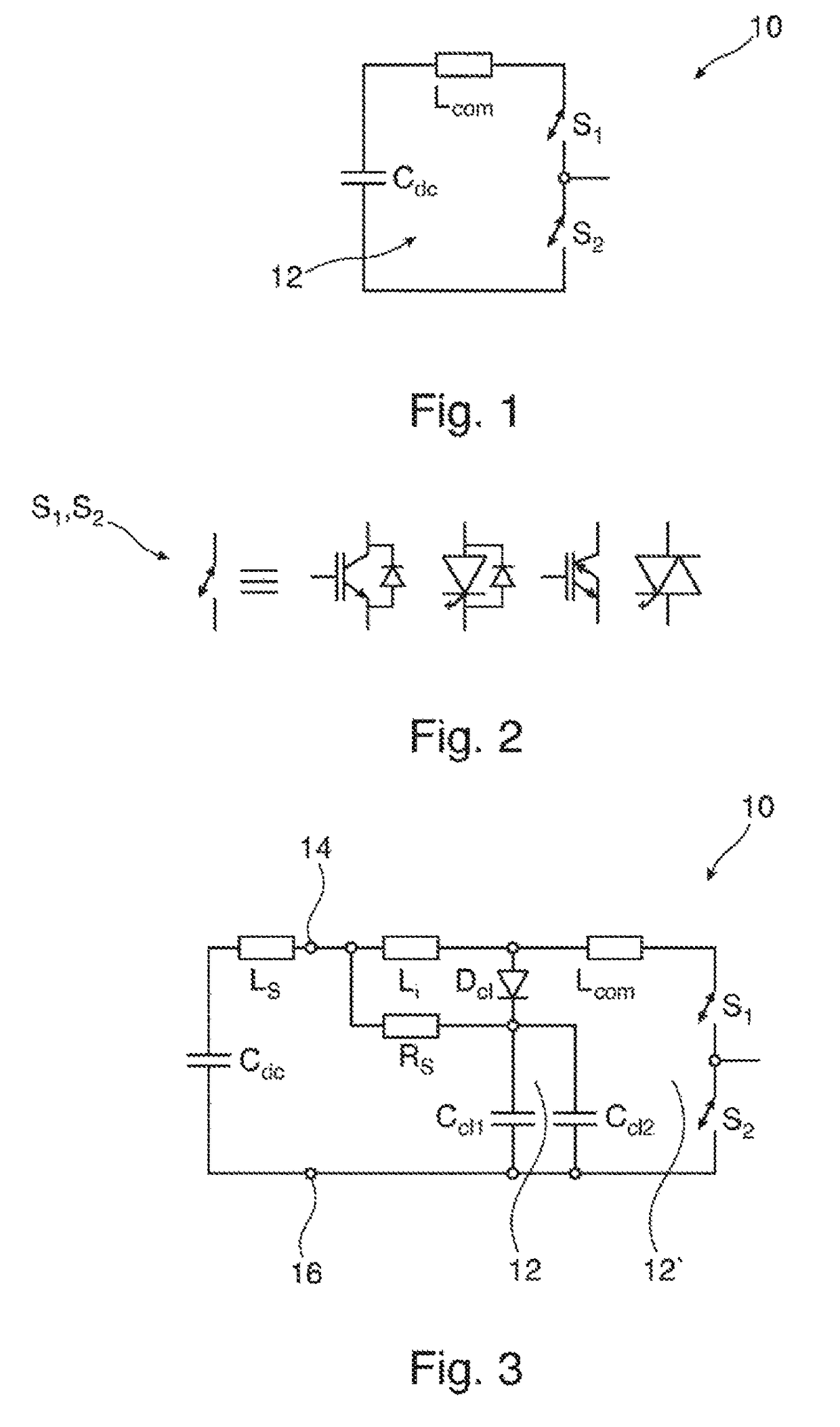
[0031]FIG. 1 schematically illustrates a two-level voltage source converter 10 comprising a commutation loop 12 between two semiconductor switches S1, S2, a capacitor Cdc being arranged in said commutation loop. Said loop 12 has a leakage inductance or commutation impedance Lcom.

[0032]If a commutation of the current occurs between the two switches, the current i does not fall abruptly owing to the leakage inductance, but rather is temporally dependent, which leads to voltage spikes that load the semiconductor switches. The overvoltage v that occurs is calculated here by v=Lcom*di / dt.

[0033]As is illustrated in FIG. 2, the semiconductor switches S1, S2 can comprise for example a transistor, thyristor, IGBT, IGCT, RC-IGBT, RC-IGCT, etc.

[0034]FIG. 3 shows a two-level converter 10 comprising further switching components in order to prevent or at least to reduce voltage spikes generated by the leakage inductance Lcom. The circuit shown in FIG. 3 is a so-called RCLD damping circuit. By way...


PUM


Abstract

A semiconductor stack for a converter comprises two series-connected semiconductor switches; two terminals for connecting a cell capacitor, which are connected to one another by the two semiconductor switches; at least one cooling element arranged between the semiconductor switches; a frame, by which the semiconductor switches and the cooling element are fixed to one another and which provides the terminals; and at least two snubber capacitors which are mechanically fixed to the frame and which are connected in parallel, are connected to the terminals and which in each case form a commutation loop with the semiconductor switches.

Description

FIELD OF THE INVENTION[0001]The invention relates to a semiconductor stack or press pack for a power converter.BACKGROUND OF THE INVENTION[0002]In many power electronic circuits, the current oscillates or commutates from one semiconductor device to another equivalent semiconductor device via a commutation loop. By way of example, two-level converters comprise two semiconductor switches which are connected to a capacitor and thus with the capacitor form a commutation loop. In general, the commutation loop has a certain leakage inductance produced, for example, by the conductors that connect the semiconductor components and by the inductance of the capacitor.[0003]If a commutation of the current occurs between the two switches, the current does not fall abruptly owing to the leakage inductance, but rather is temporally dependent, which leads to voltage spikes that load the semiconductor switches. Since each semiconductor switch can also block only a limited voltage at its inputs, a hi...

Claims


Application Information

Patent Timeline
Patent Type & Authority Patents(United States)
IPC IPC(8): H02M1/34H02M7/00H01L29/74H01L29/739H01L23/495H01L25/07H01L25/11H01L29/749H02M7/483H01L25/16H01L23/50
CPCH02M1/34H01L23/49562H01L23/49568H01L23/49575H01L23/49589H01L25/074H01L25/117H01L29/7393H01L29/7416H02M7/003H02M2007/4835H01L23/50H01L25/16H01L29/749H01L2924/0002H01L2924/00H02M7/4835
Inventor SENTURK, OSMANSTEIMER, PETER
Owner HITACHI ENERGY LTD
Why Eureka
Try Eureka