
Single image detection

a single image and detection method technology, applied in image enhancement, instruments, image data processing, etc., can solve the problems of introducing noise, penalizing the signal-to-noise ratio (snr), and comparison based methods will be subject to normal differences between test and reference patterns

Active Publication Date: 2019-01-22
KLA CORP
View PDF29 Cites 12 Cited by
  • Summary
  • Abstract
  • Description
  • Claims
  • Application Information

AI Technical Summary

Benefits of technology

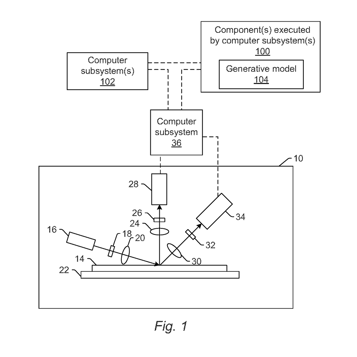
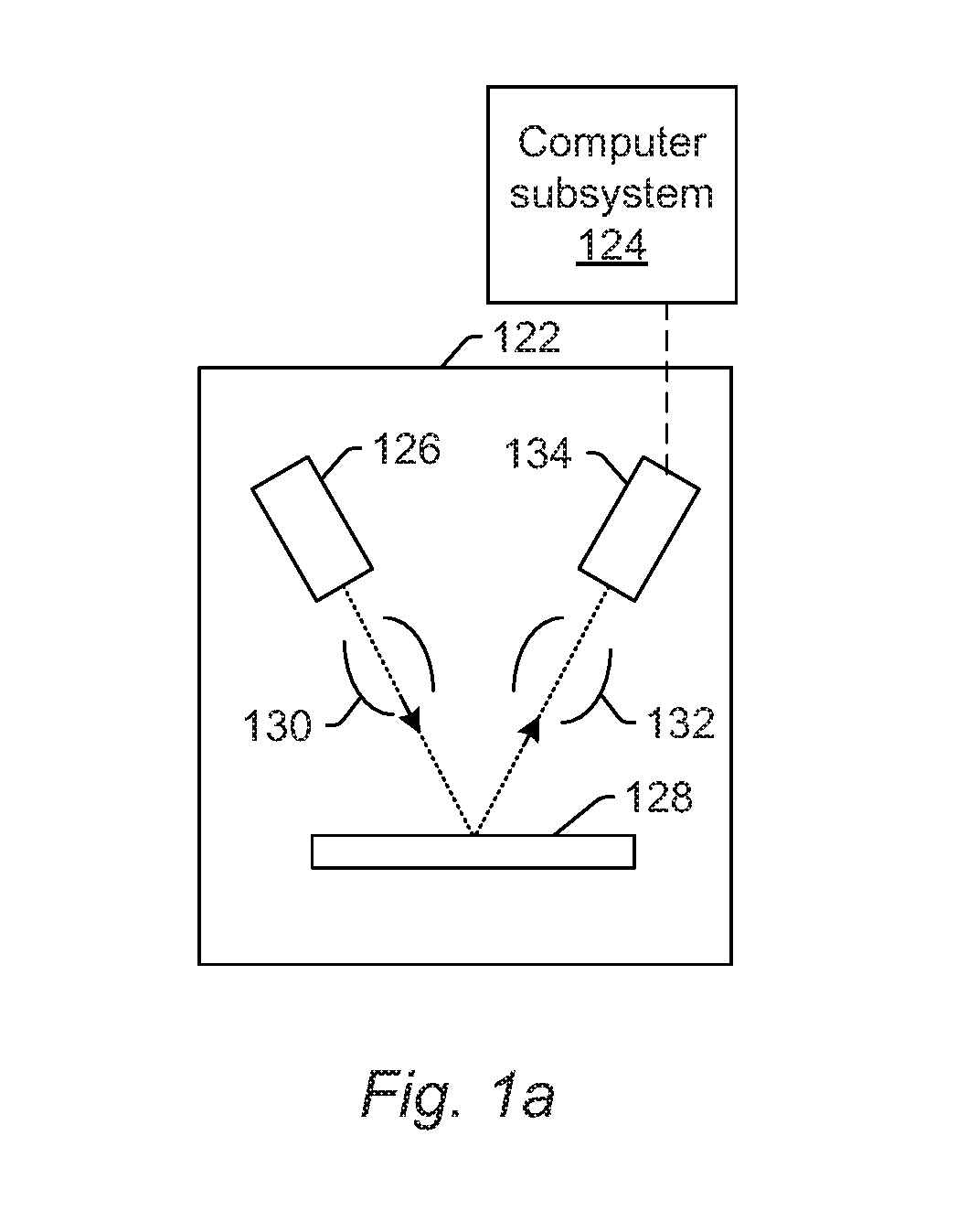
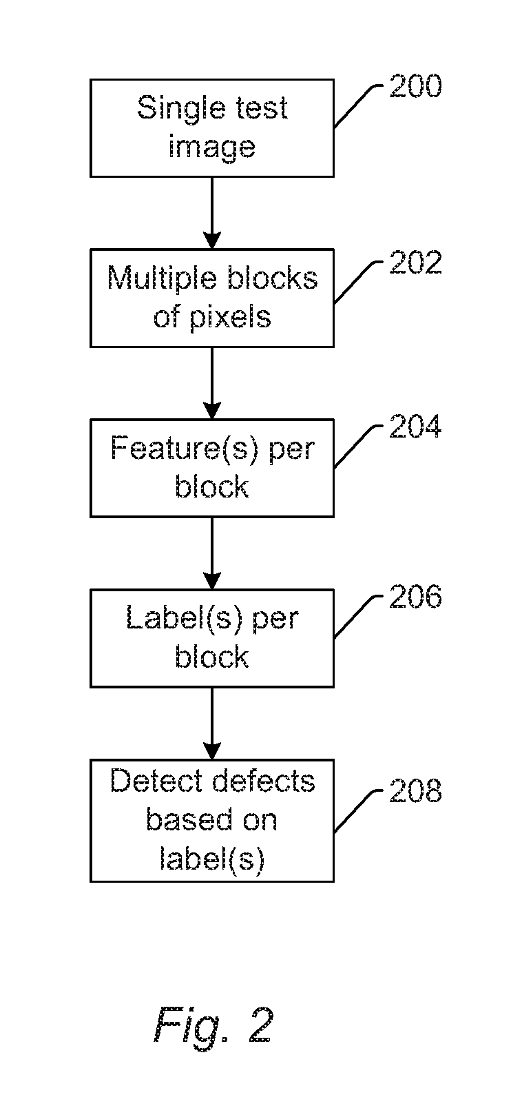
The patent describes a system and method for detecting defects on a specimen using an imaging subsystem and a generative model. The system can generate a single test image for a portion of the specimen and input it into the generative model, which separates the image into multiple blocks of pixels and determines a feature for each block based on the pixels in the block. The generative model then selects one of multiple labels for each block based on the determined feature and the mapping of the blocks into labels. The system can detect defects in the specimen based on the selected label for each block. The technical effect of this patent is a more accurate and efficient method for detecting defects on a specimen.

Problems solved by technology

However, as the dimensions of semiconductor devices decrease, inspection becomes even more important to the successful manufacture of acceptable semiconductor devices because smaller defects can cause the devices to fail.
There are, however, a number of disadvantages of the above described inspection methods.
Reference images can also introduce some noise in the analysis which always penalizes the signal-to-noise ratio (SNR).
A separate module can take care of the defect classification part, but generally leads to poor results due to defect localization issues.
Furthermore, any comparison based method will be subject to normal differences between the test and reference patterns.
Typical comparison methods limit sensitivity due to nominal LER.

Method used


Image

  • Single image detection
  • Single image detection
  • Single image detection

Examples


Embodiment Construction

[0023]The terms “design,”“design data,” and “design information” as used interchangeably herein generally refer to the physical design (layout) of an IC and data derived from the physical design through complex simulation or simple geometric and Boolean operations. In addition, an image of a reticle acquired by a reticle inspection system and / or derivatives thereof can be used as a “proxy” or “proxies” for the design. Such a reticle image or a derivative thereof can serve as a substitute for the design layout in any embodiments described herein that use a design. The design may include any other design data or design data proxies described in commonly owned U.S. Pat. No. 7,570,796 issued on Aug. 4, 2009 to Zafar et al. and U.S. Pat. No. 7,676,077 issued on Mar. 9, 2010 to Kulkarni et al., both of which are incorporated by reference as if fully set forth herein. In addition, the design data can be standard cell library data, integrated layout data, design data for one or more layers,...


PUM


Abstract

Methods and systems for detecting defects on a specimen are provided. One system includes a generative model. The generative model includes a non-linear network configured for mapping blocks of pixels of an input feature map volume into labels. The labels are indicative of one or more defect-related characteristics of the blocks. The system inputs a single test image into the generative model, which determines features of blocks of pixels in the single test image and determines labels for the blocks based on the mapping. The system detects defects on the specimen based on the determined labels.

Description

BACKGROUND OF THE INVENTION[0001]1. Field of the Invention[0002]The present invention generally relates to methods and systems for detecting defects on a specimen by single image detection.[0003]2. Description of the Related Art[0004]The following description and examples are not admitted to be prior art by virtue of their inclusion in this section.[0005]Fabricating semiconductor devices such as logic and memory devices typically includes processing a substrate such as a semiconductor wafer using a large number of semiconductor fabrication processes to form various features and multiple levels of the semiconductor devices. For example, lithography is a semiconductor fabrication process that involves transferring a pattern from a reticle to a resist arranged on a semiconductor wafer. Additional examples of semiconductor fabrication processes include, but are not limited to, chemical-mechanical polishing (CMP), etch, deposition, and ion implantation. Multiple semiconductor devices may...

Claims


Application Information

Patent Timeline
Patent Type & Authority Patents(United States)
IPC IPC(8): G06K9/00G06K9/62G06T7/00G06K9/46G06V10/50
CPCG06T7/0004G06K9/6256G06K9/6269G06K9/6287G06T2207/30148G06T2207/10061G06T2207/20021G06T2207/20081G06T2207/20084G06K9/4642G06V10/50G01N21/88G01N21/8851G01N21/956G01N2021/8858G01N2021/8893G06F18/2411G06F18/2453G06F18/214
Inventor KARSENTI, LAURENTBHASKAR, KRISJORDAN, III, JOHN RAYMONDVENKATARAMAN, SANKARCARMON, YAIR
Owner KLA CORP
Learn More