Semiconductor structure capable of improving row hammer effect in dynamic random access memory and fabrication method thereof

a technology of dynamic random access memory and semiconductor structure, applied in the field of semiconductor structure capable of improving the row hammer phenomenon, can solve the problems of row hammer phenomenon becoming more and more serious, data stored in adjacent rows of the target row is likely to be lost or interfered, and data stored in adjacent rows may be corrupted by signal crosstalk, so as to achieve the effect of improving the semiconductor structur

Active Publication Date: 2019-02-19
UNITED MICROELECTRONICS CORP +1
View PDF8 Cites 6 Cited by
  • Summary
  • Abstract
  • Description
  • Claims
  • Application Information

AI Technical Summary

Benefits of technology

[0005]The main object of the present invention is to provide an improved semiconductor structure and a method of fabricating the same to overcome the deficiencies and disadvantages of the prior art.

Problems solved by technology

When the target row of a DRAM is activated too many times over a period of time, the data stored in adjacent rows of the target row is likely to be lost or interfered with.
More specifically, the data stored in adjacent rows may be corrupted by signal crosstalk due to the frequent activation of the target row.
With the increase of DRAM design density, the phenomenon of row hammer will become more and more serious, which has become an urgent problem to be solved in this technical field.

Method used


Image

  • Semiconductor structure capable of improving row hammer effect in dynamic random access memory and fabrication method thereof
  • Semiconductor structure capable of improving row hammer effect in dynamic random access memory and fabrication method thereof
  • Semiconductor structure capable of improving row hammer effect in dynamic random access memory and fabrication method thereof

Examples


Embodiment Construction

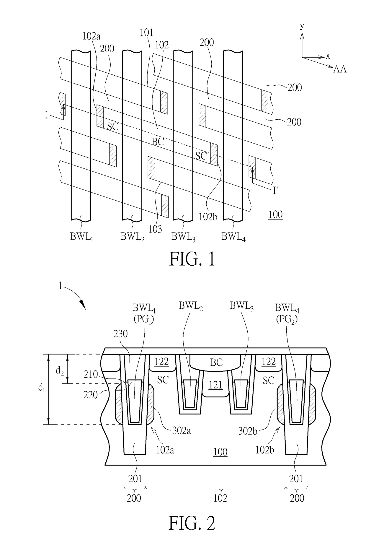
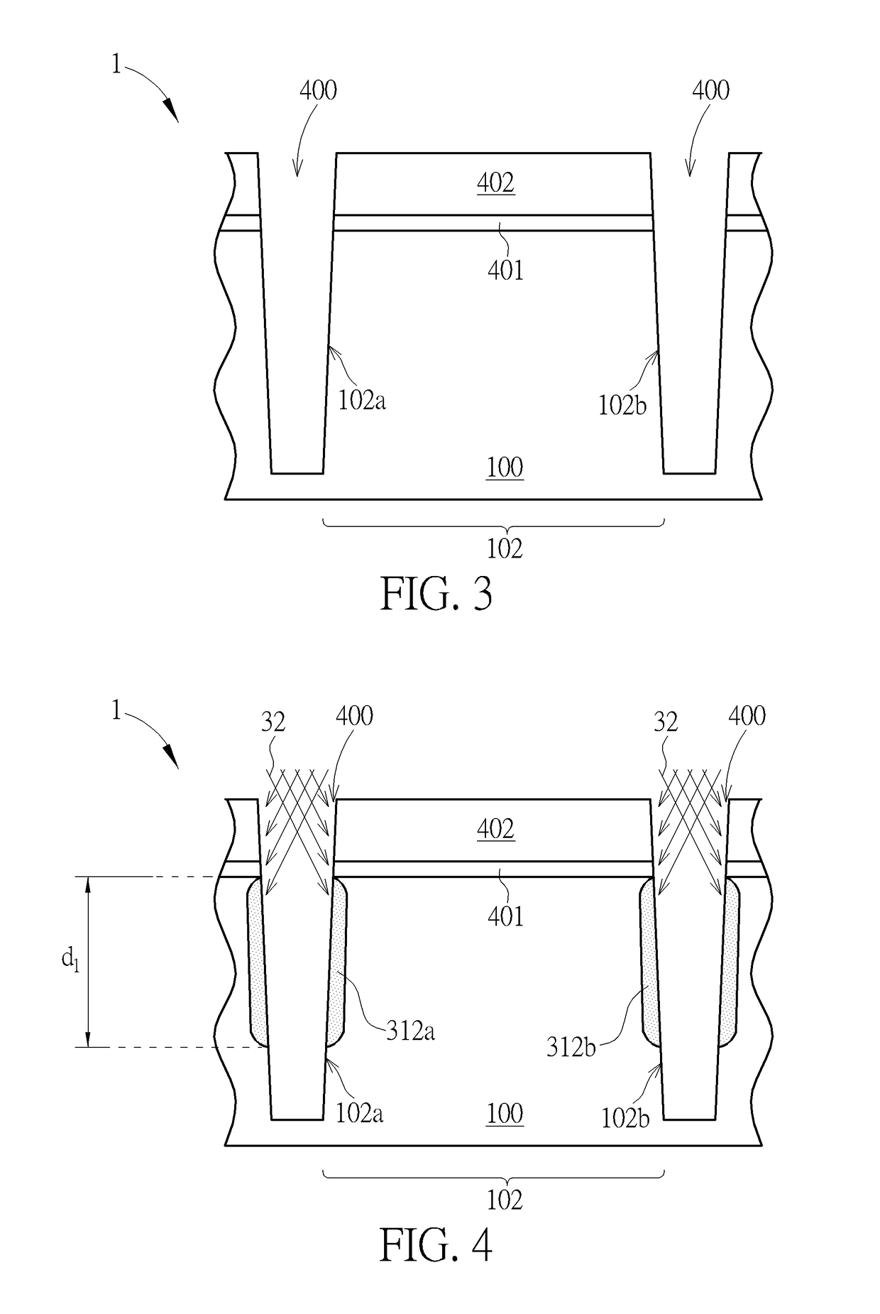
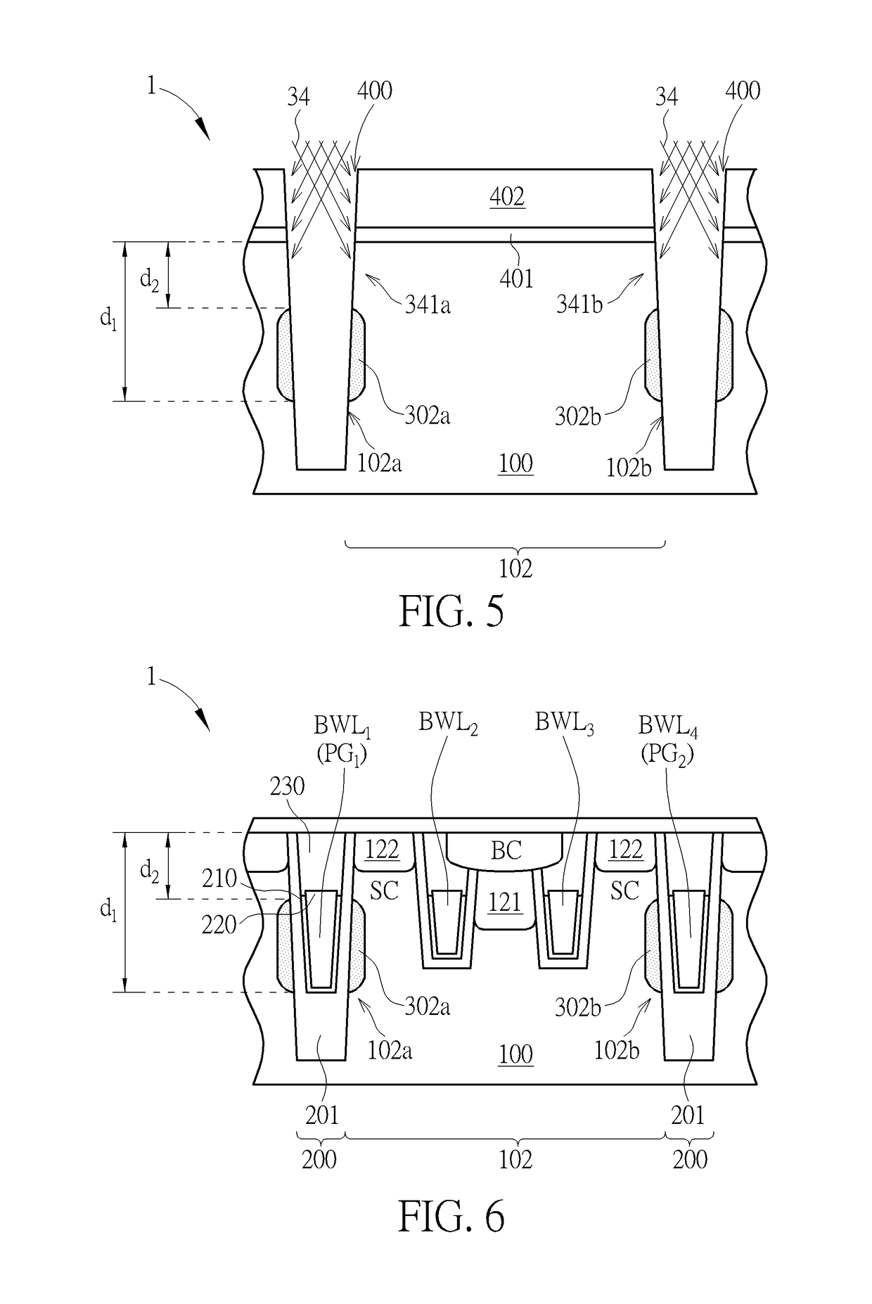
[0012]In the following detailed description of the invention, reference is made to the accompanying drawings which form a part hereof, and in which is shown, by way of illustration, specific embodiments in which the invention may be practiced. These embodiments are described in sufficient detail to enable those skilled in the art to practice the invention. Other embodiments may be utilized and structural, logical, and electrical changes may be made without departing from the scope of the present invention.

[0013]Before further describing preferred embodiments, the specific terms used throughout the specification are described below.

[0014]The term “etch” is used herein generally to describe the process of patterning a material so that at least a portion of the material after the etch is completed can be remained. For example, a method of etching silicon typically involves patterning a photoresist layer over the silicon and then removing the silicon from areas that are not protected by...


PUM


Abstract

A semiconductor structure includes a substrate with a first conductivity type and a first doping concentration, an active area with its longitudinal axis extending along a first direction, a trench isolation structure contiguous with an end surface of the active area, a passing gate in the trench isolation structure and extending along a second direction that is not parallel with the first direction, and a localized doping region with a second conductivity type and a second doping concentration that is located on the end surface.

Description

CROSS REFERENCE TO RELATED APPLICATION[0001]This application claims the priority from CN application No. 201710201850.1, filed Mar. 30, 2017, which is included in its entirety herein by reference.BACKGROUND OF THE INVENTION1. Field of the Invention[0002]The present invention relates to the field of semiconductor technology, and more particularly, to a semiconductor structure capable of improving the row hammer phenomenon of a dynamic random access memory (DRAM) and a method of fabricating the same.2. Description of the Prior Art[0003]When the target row of a DRAM is activated too many times over a period of time, the data stored in adjacent rows of the target row is likely to be lost or interfered with. More specifically, the data stored in adjacent rows may be corrupted by signal crosstalk due to the frequent activation of the target row. This phenomenon is also called “row hammer”.[0004]With the increase of DRAM design density, the phenomenon of row hammer will become more and mor...

Claims


Application Information

Patent Timeline
Patent Type & Authority Patents(United States)
IPC IPC(8): H01L29/06H01L21/761H01L21/8234H01L21/762H01L27/108
CPCH01L21/761H01L21/76224H01L21/823481H01L27/10876H01L27/10891H01L29/0649H01L27/10814H01L2924/14H10B12/02H10B12/30H01L21/823437H10B12/05H10B12/053H10B12/488H10B12/315
Inventor NAGAI, YUKIHIRO
Owner UNITED MICROELECTRONICS CORP
Why Eureka
Try Eureka