Liquid crystal display device and manufacture method thereof

a technology of liquid crystal display and manufacturing method, which is applied in the direction of optical elements, instruments, coatings, etc., can solve the problems of narrow temperature range, difficult to be utilized in practical application, and difficult to recover to the initial state after recovery, so as to reduce temperature precision and the difficulty of polymerization process, improve the hysteresis, and improve the backlight efficiency and display color gamut

Active Publication Date: 2019-03-05
TCL CHINA STAR OPTOELECTRONICS TECH CO LTD
View PDF9 Cites 6 Cited by
  • Summary
  • Abstract
  • Description
  • Claims
  • Application Information

AI Technical Summary

Benefits of technology

[0007]An objective of the present invention is to provides a liquid crystal display device, which is a blue phase liquid crystal display device without the alignment layers, and the manufacture cost is low, and the response is fast, and the backlight efficiency is high, and the display color gamut is high, which can be applied for the rapid display and 3D display fields.
[0008]Another objective of the present invention is to provide a manufacture method of a liquid crystal display device, which reduce the manufacture cost, and promote the response speed, the backlight efficiency and the display color gamut of the liquid crystal display device.
[0046]The benefits of the present invention are: the liquid crystal display device provided by the present invention is a blue phase liquid crystal display device. The alignment layer is not required. The liquid crystal composition forming the liquid crystal layer comprises liquid crystal material, quantum dots material mixed in the liquid crystal material, polymeric monomer and chiral material; the polymeric monomer is polymerized to form a polymer network under a blue phase temperature range of the liquid crystal material as forming the liquid crystal layer, which can stabilize the blue phase liquid crystal, and thus to expand the blue phase temperature range of the liquid crystal material. The grain size of the quantum dots material in the liquid crystal composition is in the nano scale, which can expand the blue phase liquid crystal temperature range. Namely, the blue phase temperature range of the liquid crystal material has already been expanded before the polymeric monomer is polymerized. Thus, the temperature precision requirement and the difficulty of the polymerization process is decreased, and the quantum dots material can improve the hysteresis, and meanwhile raise the backlight efficiency and the display color gamut of the liquid crystal display device, and the liquid crystal display device can be applied for the rapid display and 3D display fields. In the manufacture method of the liquid crystal display device, the liquid crystal composition forming the liquid crystal layer comprises liquid crystal material, quantum dots material mixed in the liquid crystal material, polymeric monomer and chiral material, and as the liquid crystal material is in the blue phase temperature range, the ultraviolet irradiation is implemented to the polymeric monomer to polymerize the same to form a polymer network, and thus to form the blue phase liquid crystal display device having wide temperature range, low hysteresis effect. The manufacture of the alignment layer in the liquid crystal display device can be eliminated to reduce the cost to raise the response speed of the liquid crystal display device and to raise the backlight efficiency and the display color gamut of the liquid crystal display device.

Problems solved by technology

However, there is the issue that the temperature range is narrow (1-2° C.
), and the driving voltage is high, and it is difficult to recovery to the initial state after the electrical power is applied, i.e. the hysteresis for the blue phase liquid crystal.
IT is hard to be utilized in the practical application.

Method used


Image

  • Liquid crystal display device and manufacture method thereof
  • Liquid crystal display device and manufacture method thereof
  • Liquid crystal display device and manufacture method thereof

Examples


Embodiment Construction

[0055]For better explaining the technical solution and the effect of the present invention, the present invention will be further described in detail with the accompanying drawings and the specific embodiments.

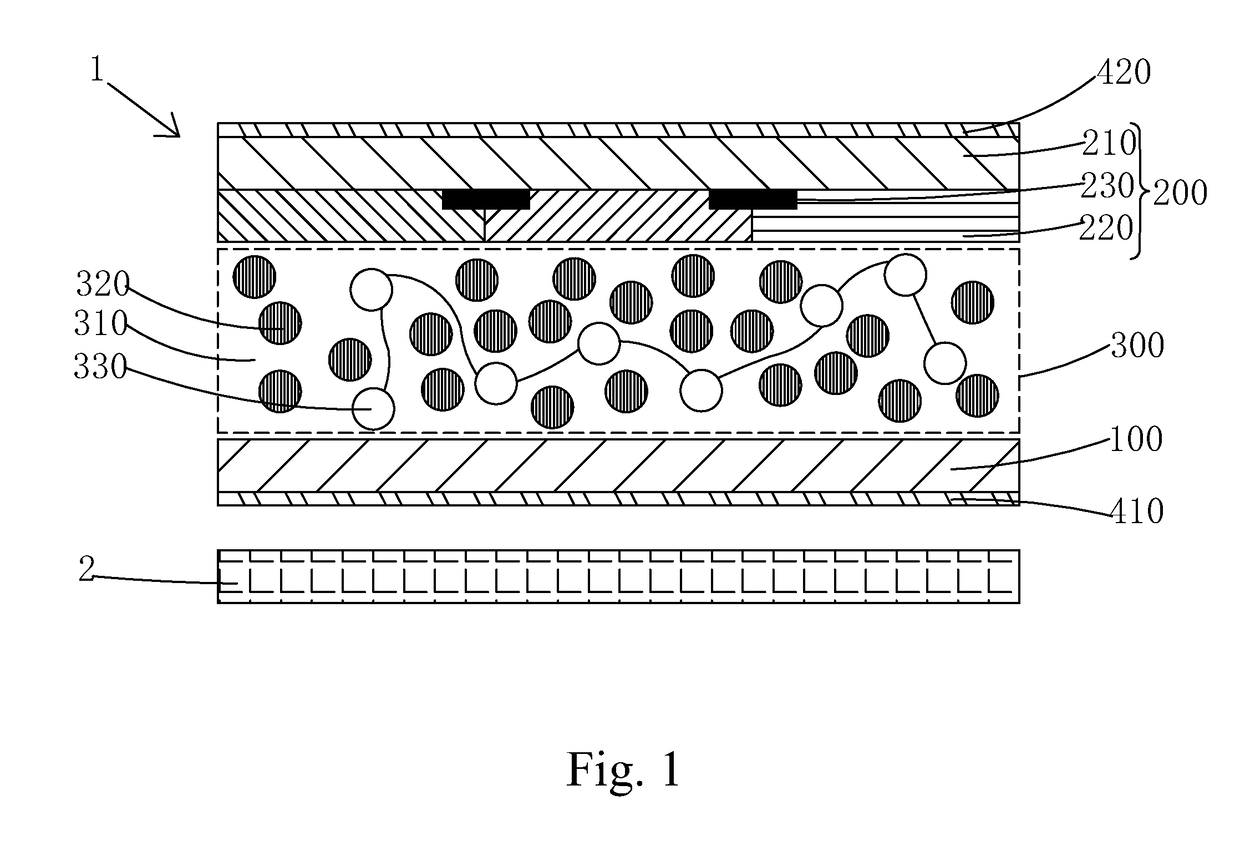
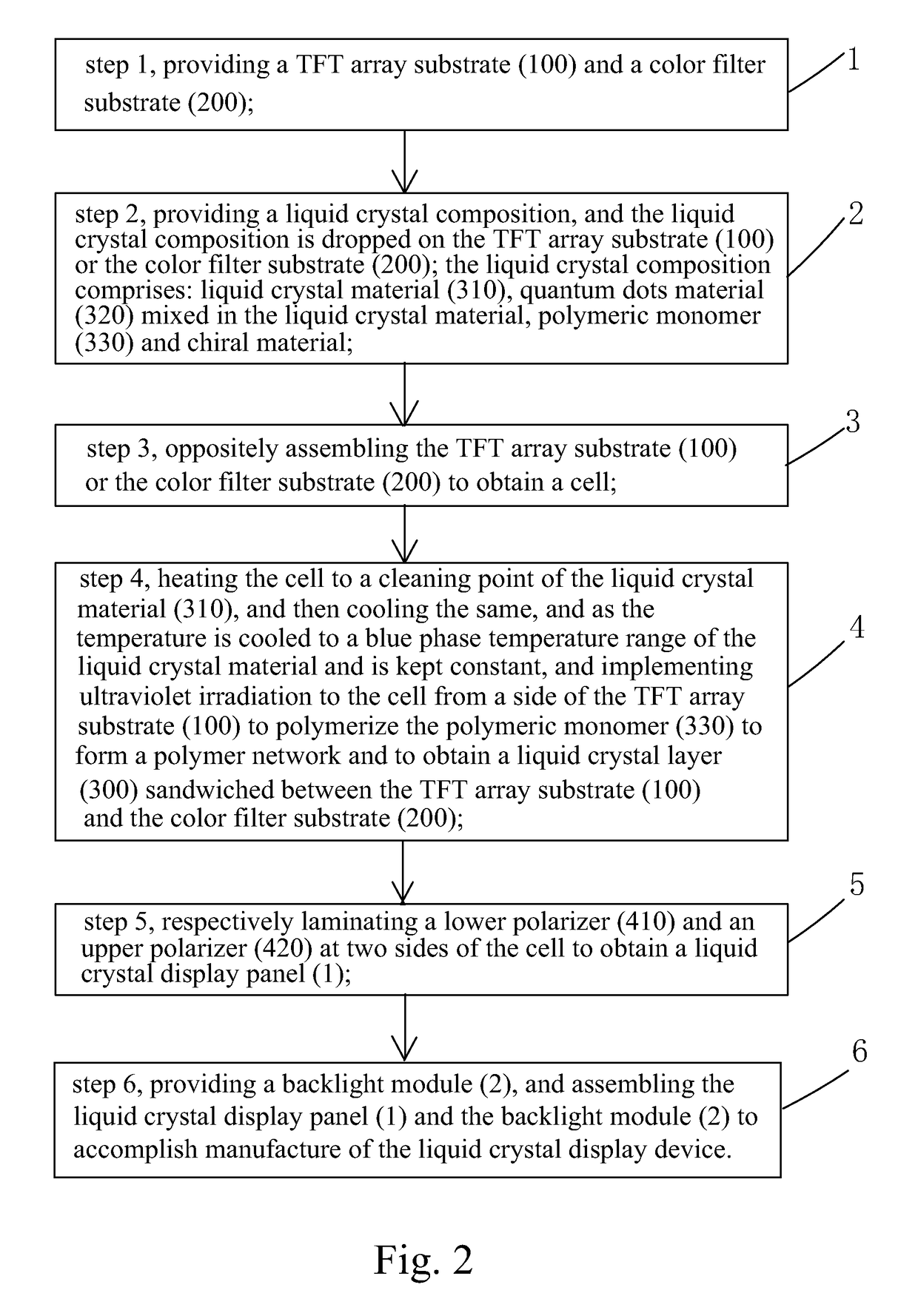
[0056]Please refer to FIG. 1. The present invention provides a liquid crystal display device, comprising a liquid crystal display panel 1 and a backlight module 2 under the liquid crystal display panel 1;

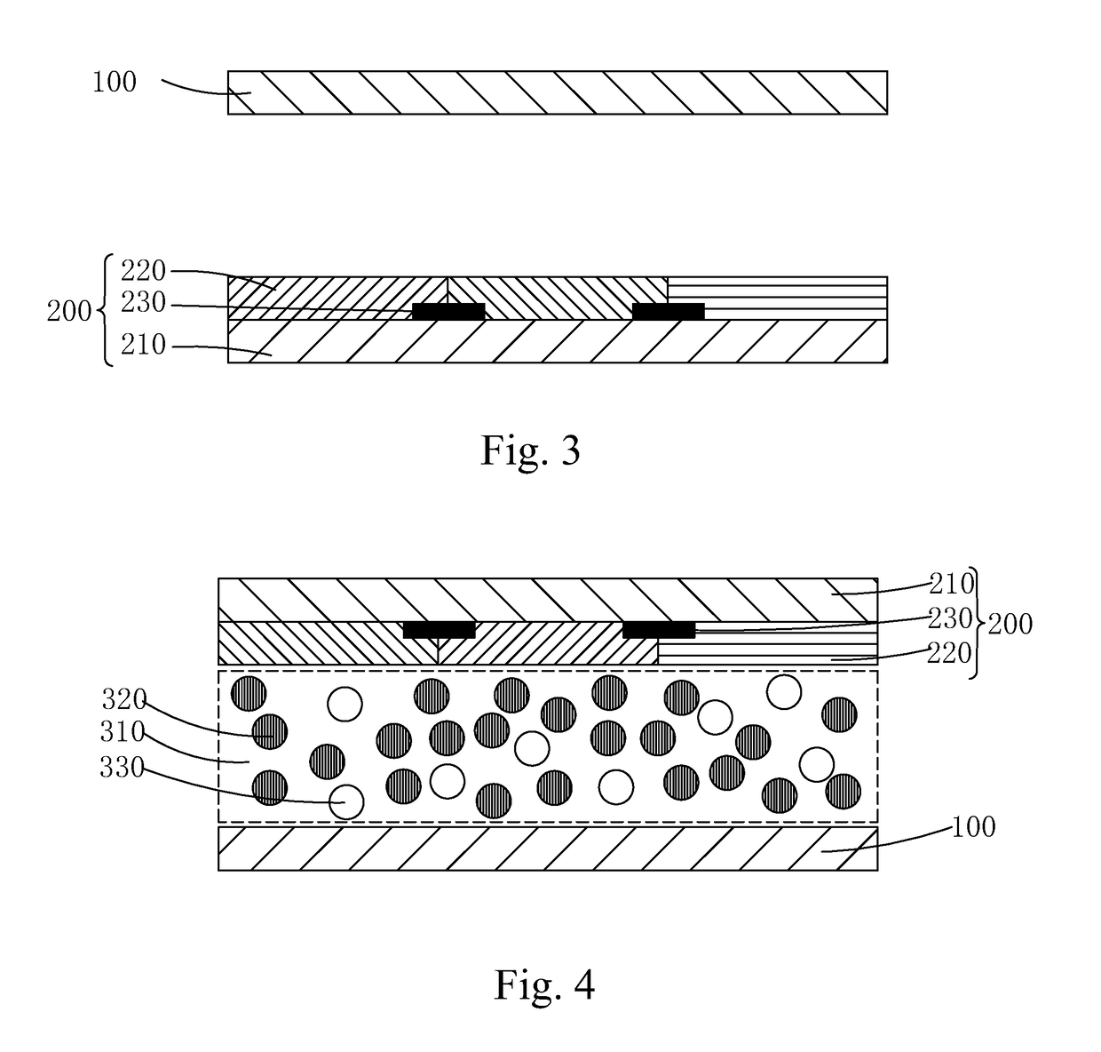
[0057]the liquid crystal display panel 1 comprises a TFT array substrate 100 and a color filter substrate 200 which are oppositely located, and a liquid crystal layer 300 sandwiched between the TFT array substrate 100 and the color filter substrate 200, a lower polarizer 410 located at one side of the TFT array substrate 100 away from the liquid crystal layer 300 and an upper polarizer 420 located at one side of the color filter substrate 200 away from the liquid crystal layer 300.

[0058]The TFT array substrate 100 comprises: a first substrate, a TFT array located on the first ...


PUM

PropertyMeasurementUnit
sizesaaaaaaaaaa
grain sizesaaaaaaaaaa
temperatureaaaaaaaaaa

Abstract

Provided are a liquid crystal display device and a manufacture method thereof. The liquid crystal display device is a blue phase liquid crystal display device. The alignment layer is not required. The liquid crystal composition forming the liquid crystal layer comprises liquid crystal material, quantum dots material mixed in the liquid crystal material, polymeric monomer and chiral material; the polymeric monomer is polymerized to form a polymer network under a blue phase temperature range as forming the liquid crystal layer, which can stabilize the blue phase liquid crystal, and thus to expand the blue phase temperature range. The grain size of the quantum dots material in the liquid crystal composition is in the nano scale, which can expand the blue phase liquid crystal temperature range. Namely, the blue phase temperature range of the liquid crystal material has already been expanded before the polymeric monomer is polymerized.

Description

FIELD OF THE INVENTION[0001]The present invention relates to a liquid crystal display technology field, and more particularly to a liquid crystal display device and a manufacture method thereof.BACKGROUND OF THE INVENTION[0002]The Liquid Crystal Display (LCD) is one of the most widely utilized flat panel displays, and the liquid crystal display panel is the core component of the Liquid Crystal Display.[0003]The traditional liquid crystal display panel generally comprises a Color Filter (CF), a Thin Film Transistor Array Substrate (TFT Array Substrate) and a Liquid Crystal Layer positioned inbetween. The working principle is that the liquid crystal molecules are positioned between the two parallel glass substrates, and many vertical and horizontal tiny little electrical lines are between the two glass substrates, and the light of backlight module is reflected to generate images by applying driving voltages or not for controlling the direction changes of the liquid crystal molecules. ...

Claims


Application Information

Patent Timeline
Patent Type & Authority Patents(United States)
IPC IPC(8): C09K19/54G02F1/1335C09K19/02C09K19/58G02B27/22C09K11/02G02F1/1368G02F1/1339C08F122/20C09K19/52G02F1/137C09K19/30C09K19/04G02B30/00
CPCG02F1/1368C09K11/025C09K19/0275C09K19/542C09K19/586G02B27/22G02F1/133512G02F1/133528G02F1/133617G02F1/133621C08F122/20G02F2202/36C09K2019/0448C09K2019/301C09K2019/3004C09K2019/3009C09K2019/521C09K2019/546G02F1/13394G02F1/133514G02F2001/13793G02F2001/133614G02F2202/022G02F1/1333G02F1/137G02F1/13793G02F1/13775C09D4/00G02F1/133614
Inventor CHEN, XINGWUMA, XIAOLONG
Owner TCL CHINA STAR OPTOELECTRONICS TECH CO LTD
Why Eureka
Try Eureka