Moisture-resistant chip scale packaging light-emitting device

a chip scale and packaging technology, applied in the field of light-emitting devices, can solve the problems of reducing affecting the light intensity of the light source, so as to prevent or minimize the effect of oxygen and moisture and small form factor

Active Publication Date: 2019-03-12
MAVEN OPTRONICS CO LTD
View PDF32 Cites 5 Cited by
  • Summary
  • Abstract
  • Description
  • Claims
  • Application Information

AI Technical Summary

Benefits of technology

[0011]One object according to some embodiments of the present disclosure is to provide light-emitting devices specified with moisture barrier structures to prevent or minimize oxygen and moisture from contacting moisture-sensitive photoluminescent materials used inside the light-emitting devices. Desirably, the embodiments of the moisture barrier structures do not significantly increase a package size of a light-emitting device, so that a chip scale packaging light-emitting device maintains the advantage of a small form factor.
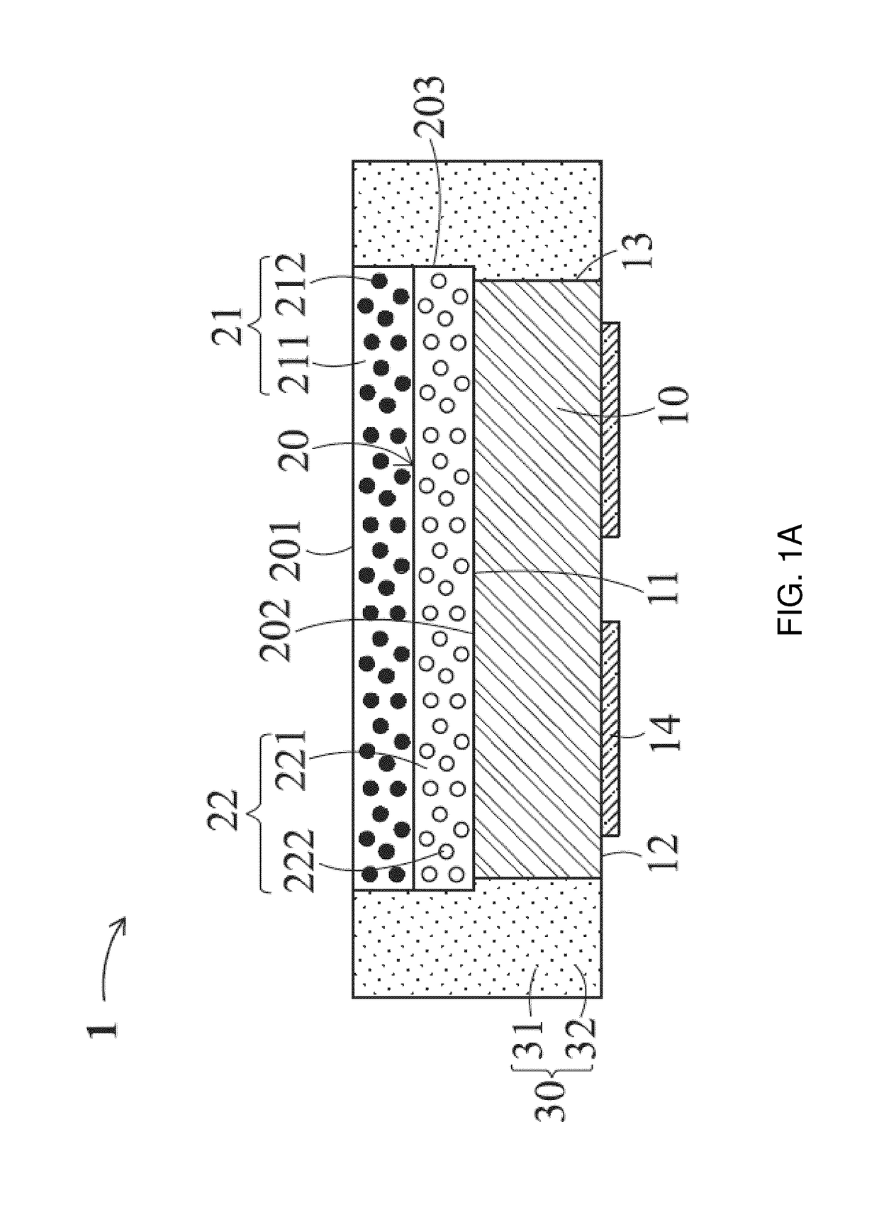
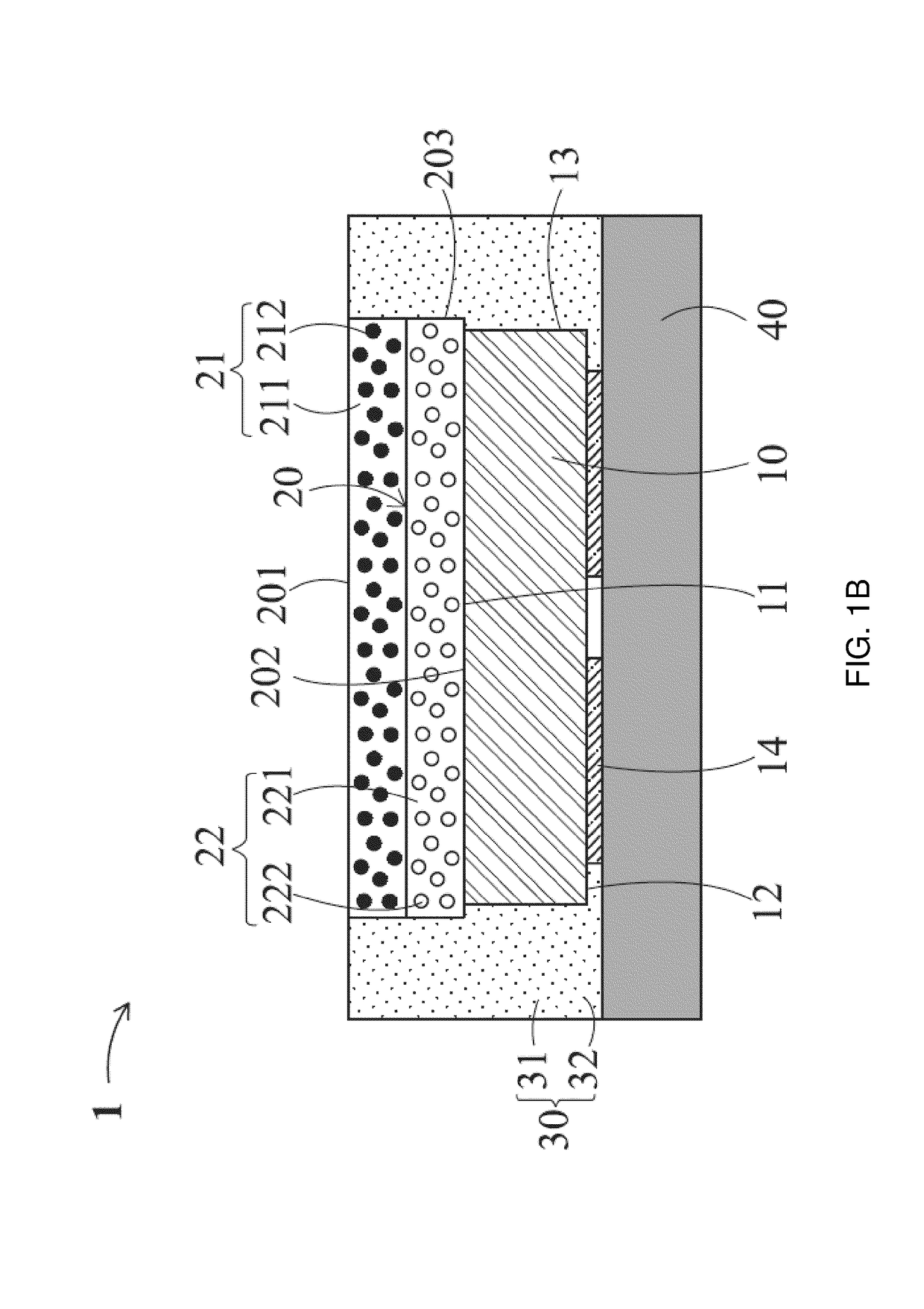
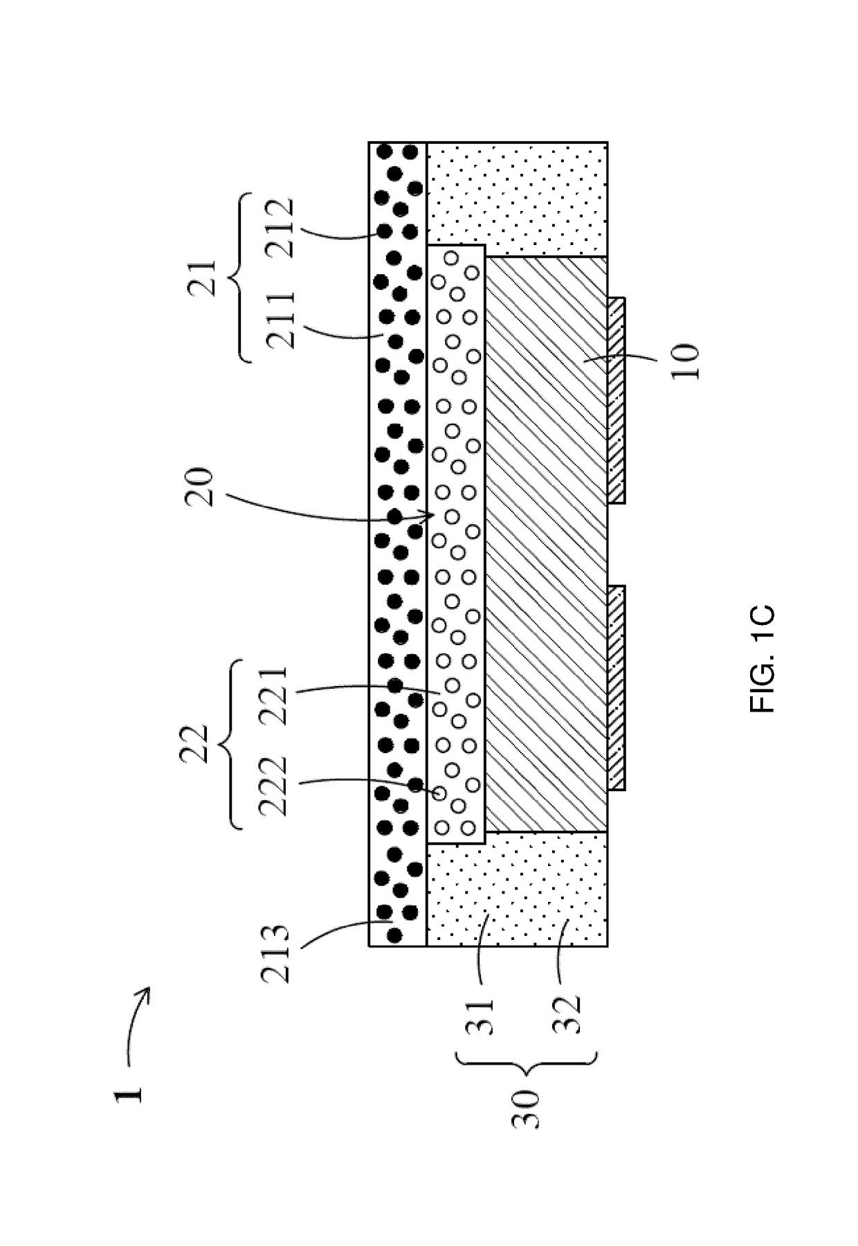
[0015]Therefore, the present disclosure provides at least the following technical advantages according to some embodiments. The first photoluminescent layer comprising the less-moisture-sensitive photoluminescent material functions as a barrier layer protecting the underneath second photoluminescent layer comprising the moisture-sensitive photoluminescent material from the ambient oxygen and moisture. The reflective structure, the encapsulation structure, and the packaging structure can also prevent outside oxygen and moisture from permeating inside so that the degradation process of the moisture-sensitive photoluminescent material is significantly reduced. In other words, the less-moisture-sensitive photoluminescent layer functions as a light-conversion layer as well as a protective barrier layer for the underneath moisture-sensitive photoluminescent layer.

Problems solved by technology

However, these photoluminescent materials are susceptible to oxygen or moisture.
The oxidized activator will cause the photoluminescent materials to become de-activated so that these photoluminescent materials gradually lose the capability of wavelength conversion, and thus gradually degrade the specified brightness or causing color spectrum shifting during its specified operation lifetime.
The above solutions may slow down the degradation process of the fluoride photoluminescent material caused by oxygen or moisture; however, this degradation still cannot be completely avoided.
Also, it is quite difficult to completely cover each of fluoride photoluminescent material particles with Manganese-free or with low-concentration Manganese layers, which will also increase phosphor fabrication cost.
Besides, the presence of the encapsulation layer will also decrease the light conversion efficiency of fluoride photoluminescent materials.
However, excessive defects and dangling bonds on the surface of the QDs may lead to non-radiative electron-hole recombinations causing relatively low quantum efficiency.
Moreover, the surface of QDs tends to be oxidized due to photochemical reaction when the QDs come into contact with oxygen or moisture.
However, similar to fluoride phosphor materials, degradation of QDs can be slowed down by using the core / shell structure, but cannot be completely avoided.
However, using the lead frame as an enclosure or housing will increase the package size of the LED.
Moreover using a thicker silicone over-layer or more amount of silicone to improve the barrier property will further enlarge the overall size of the LED.
Therefore, such solutions are unfavorable for some electronic products embedded with the LEDs, because these electronic products continue moving toward thinner and more compact in size, such as LED backlights for portable electronic devices or LED TVs.
However, a size constraint of the LED makes it even more difficult to prevent external oxygen and moisture from penetrating into an LED package.

Method used


Image

  • Moisture-resistant chip scale packaging light-emitting device
  • Moisture-resistant chip scale packaging light-emitting device
  • Moisture-resistant chip scale packaging light-emitting device

Examples


Embodiment Construction

Definitions

[0025]The following definitions apply to some of the technical aspects described with respect to some embodiments of the invention. These definitions may likewise be expanded upon herein.

[0026]As used herein, the singular terms “a,”“an,” and “the” include plural referents unless the context clearly dictates otherwise. Thus, for example, reference to a layer can include multiple layers unless the context clearly dictates otherwise.

[0027]As used herein, the term “set” refers to a collection of one or more components. Thus, for example, a set of layers can include a single layer or multiple layers. Components of a set also can be referred to as members of the set. Components of a set can be the same or different. In some instances, components of a set can share one or more common characteristics.

[0028]As used herein, the term “adjacent” refers to being near or adjoining. Adjacent components can be spaced apart from one another or can be in actual or direct contact with one a...


PUM


Abstract

A chip scale packaging (CSP) light-emitting device including a light-emitting semiconductor die and a layer-by-layer photoluminescent (PL) structure disposed on the light-emitting semiconductor die is disclosed. The PL structure includes a second PL layer and a first PL layer disposed over the second PL layer, wherein the first PL layer functions as a photoluminescent layer and a barrier layer protecting the second PL from ambient oxygen and moisture. The first PL layer includes a less-moisture-sensitive PL material dispersed within a first polymer matrix material, whereas the second PL layer includes a moisture-sensitive PL material dispersed within a second polymer material. With these arrangements, the outermost first PL layer comprising the less-moisture-sensitive photoluminescent material functions as a wavelength-conversion layer and also serves as a barrier layer protecting the inner second PL layer comprising the moisture-sensitive photoluminescent material from ambient oxygen and moisture. Thus degradation of moisture-sensitive PL material can be reduced.

Description

CROSS-REFERENCES TO RELATED APPLICATIONS[0001]This application claims the benefit of and priority to Taiwan Patent Application No. 105124965 filed on Aug. 5, 2016, and Chinese Patent Application No. 201610648426.7 filed on Aug. 9, 2016, the disclosures of which are incorporated herein by reference in their entirety.BACKGROUNDTechnical Field[0002]The present disclosure relates to a light-emitting device and, in particular, to an oxygen and moisture-resistant chip scale packaging light-emitting device including a light-emitting semiconductor die which generates electromagnetic radiation while it is in operation.Description of the Related Art[0003]Light-emitting devices (LEDs) are widely used in various applications such as general lightings, backlight units, traffic lights, portable devices, automotive lightings and so forth. Generally, a light-emitting semiconductor die is disposed inside a packaging structure, such as a lead frame, to form a packaged LED. Photoluminescent materials ...

Claims


Application Information

Patent Timeline
Patent Type & Authority Patents(United States)
IPC IPC(8): H01L33/00H01L33/60H01L33/50H01L33/54H01L33/56H01L33/44H01L33/48H01L33/36
CPCH01L33/56H01L33/504H01L33/505H01L33/507H01L33/54H01L33/60H01L2933/0091H01L33/44H01L33/486H01L33/501H01L2933/005H01L2933/0041H01L2933/0058H01L33/36
Inventor CHEN, CHIEH
Owner MAVEN OPTRONICS CO LTD
Why Eureka
Try Eureka