Method of forming metal interconnection and method of fabricating semiconductor apparatus using the method

a technology of metal interconnection and semiconductor apparatus, which is applied in the direction of semiconductor devices, semiconductor/solid-state device details, electrical devices, etc., can solve the problem of preventing moisture or water from entering the sub-layer low-k film, and achieve excellent hermetic properties

Active Publication Date: 2019-04-02
ASM IP HLDG BV
View PDF2775 Cites 279 Cited by
  • Summary
  • Abstract
  • Description
  • Claims
  • Application Information

AI Technical Summary

Benefits of technology

[0005]One or more embodiments include a method of depositing a thin film with a thickness that is less than that of an existing capping layer (i.e., a SiCN layer) and excellent hermetic properties for protecting a sub-layer low-k layer from water or moisture.

Problems solved by technology

However, the thinner SiCN film (e.g. with a thickness less than 100 Å) results in a limitation in preventing moisture or water from penetrating into a sub-layer low-k film (due to the limitation of a dielectric constant, etc.).

Method used


Image

  • Method of forming metal interconnection and method of fabricating semiconductor apparatus using the method
  • Method of forming metal interconnection and method of fabricating semiconductor apparatus using the method
  • Method of forming metal interconnection and method of fabricating semiconductor apparatus using the method

Examples


Embodiment Construction

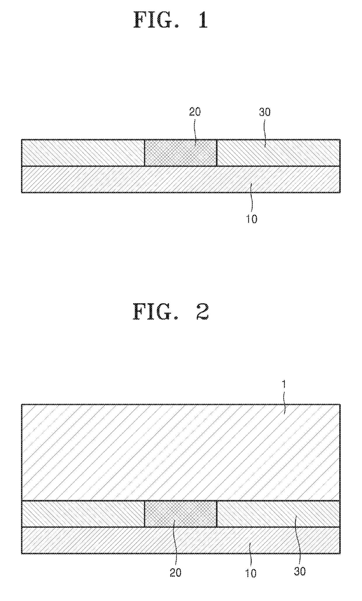
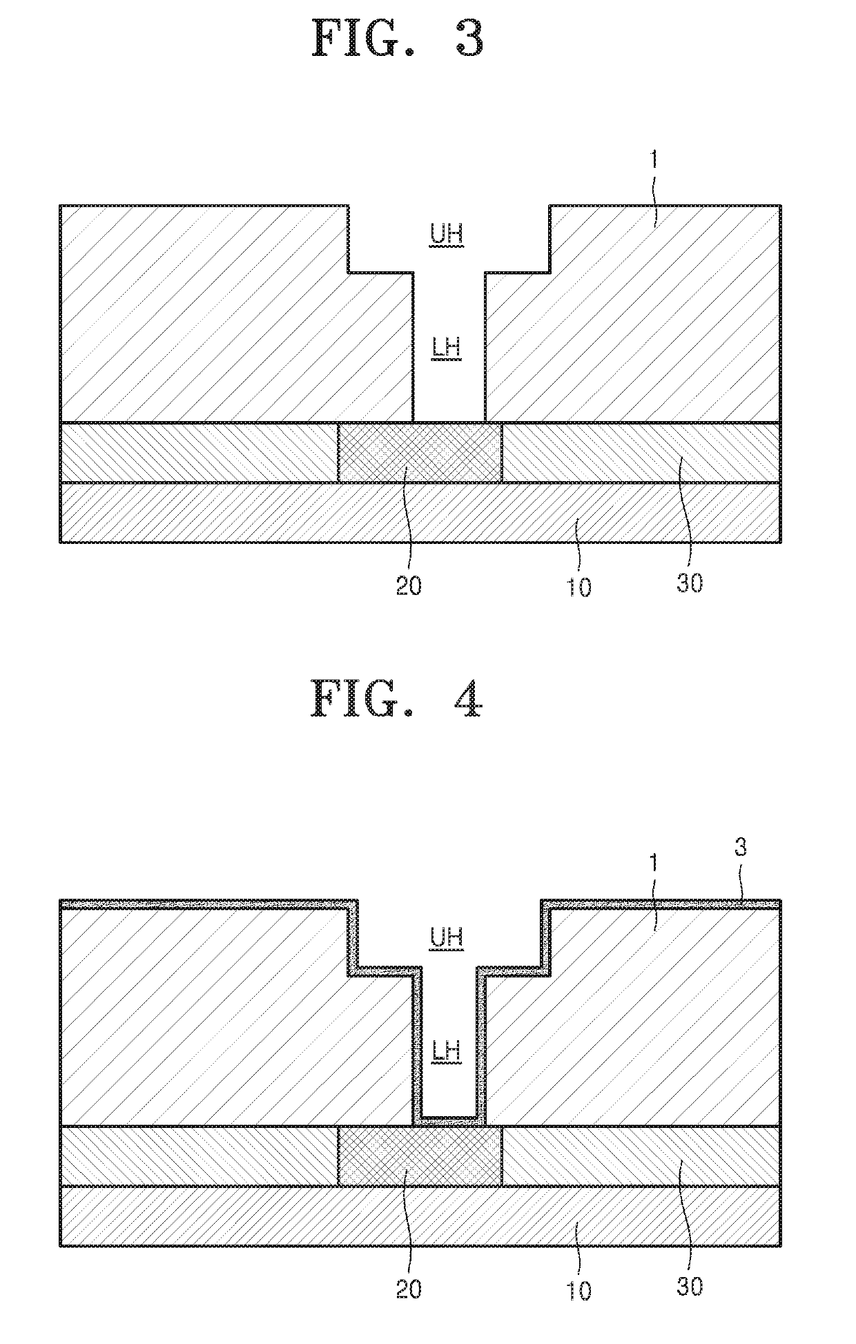
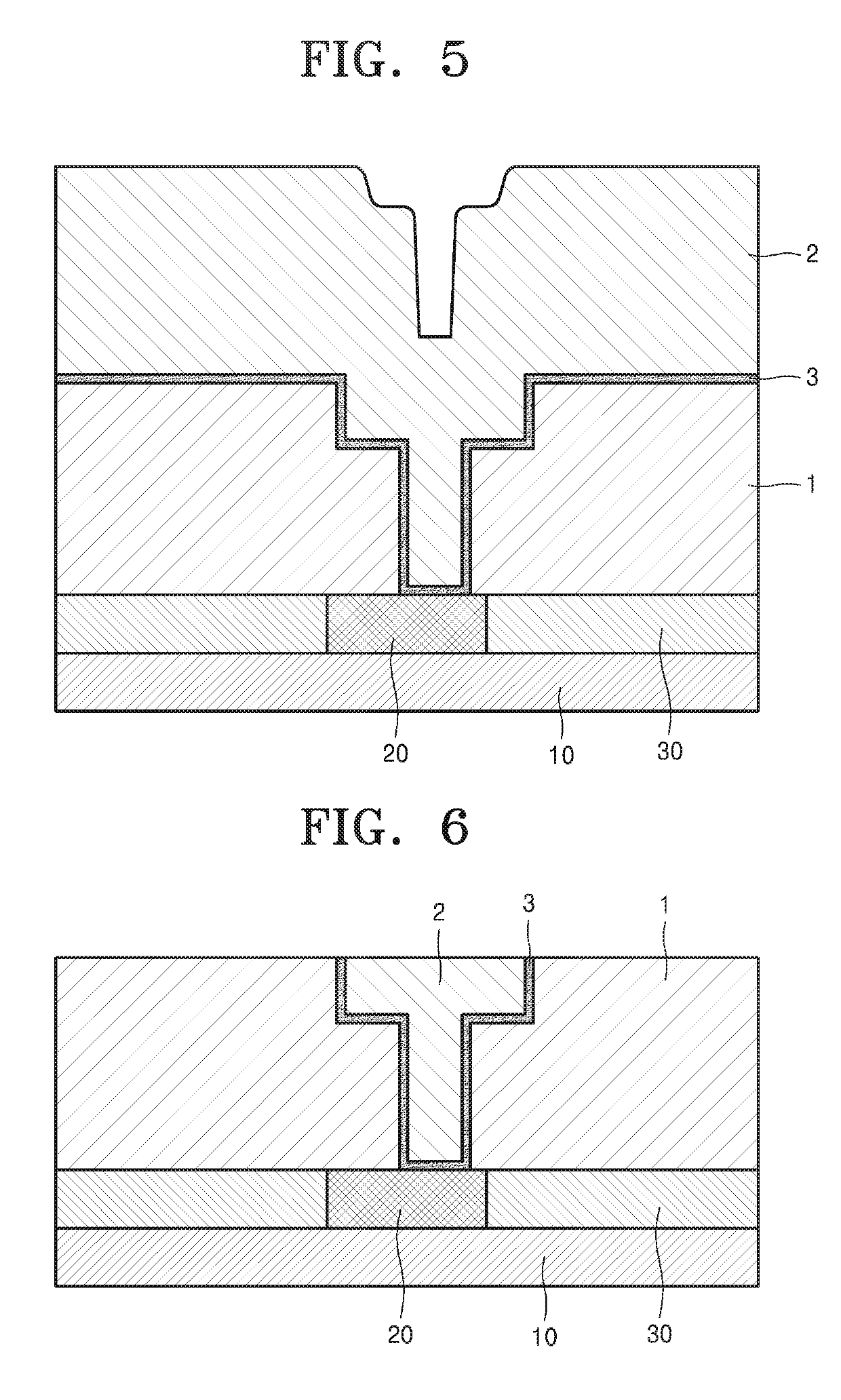
[0031]The present disclosure will now be described more fully with reference to the accompanying drawings, in which embodiments of the present disclosure are shown.

[0032]The present disclosure now will be described more fully hereinafter with reference to the accompanying drawings. The present disclosure may, however, be embodied in many different forms and should not be construed as limited to the embodiments set forth herein. Rather, these embodiments are provided so that this disclosure will be thorough and complete, and will fully convey the scope of the present disclosure to one of ordinary skill in the art.

[0033]The terminology used herein is for the purpose of describing embodiments only and is not intended to be limiting of embodiments of the present disclosure. As used herein, the singular forms “a”, “an”, and “the” are intended to include the plural forms as well, unless the context clearly indicates otherwise. It will be further understood that the terms “comprises”, “com...


PUM

PropertyMeasurementUnit
humidityaaaaaaaaaa
temperatureaaaaaaaaaa

Abstract

A semiconductor manufacturing method includes depositing a low-k dielectric layer, forming a trench in the low-k dielectric layer, forming a barrier layer in the trench, filling a metal on the barrier layer, planarizing the metal, and forming a capping layer on the planarized metal, wherein the capping layer includes at least two layers.

Description

CROSS-REFERENCE TO RELATED APPLICATION[0001]This application claims the benefit of Korean Patent Application No. 10-2016-0060210, filed on May 17, 2016, in the Korean Intellectual Property Office, the disclosure of which is incorporated herein in its entirety by reference.BACKGROUND1. Field[0002]One or more embodiments relate to a method of forming a metal interconnection and a method of fabricating a semiconductor device in the semiconductor device manufacturing apparatus using the method.2. Description of the Related Art[0003]As the size of semiconductor device shrinks, a response time of the semiconductor device slows down due to line resistances of metal interconnections in wiring structures and dielectric constants of interlayer dielectric layers that surround the metal interconnections. Such problems are referred to as resistance-capacitance (RC) delay. In order to reduce RC delay, materials of the metal interconnections are changed from aluminum to copper with a resistance lo...

Claims


Application Information

Patent Timeline
Patent Type & Authority Patents(United States)
IPC IPC(8): H01L21/4763H01L21/768H01L23/00H01L21/02H01L23/532H01L23/522
CPCH01L23/564H01L21/0228H01L21/02178H01L21/02211H01L21/02219H01L21/02274H01L21/7684H01L21/76802H01L21/76832H01L21/76834H01L21/76843H01L21/76877H01L23/5226H01L23/53238H01L23/53295H01L21/0217H01L21/02074H01L21/76838H01L21/76816H01L21/76831H01L21/76841H01L21/76856
Inventor LEE, CHOONG MANYOO, YONG MINKIM, YOUNG JAECHUN, SEUNG JUKIM, SUN JA
Owner ASM IP HLDG BV
Why Eureka
Try Eureka