Solid-state imaging element, imaging device, and electronic apparatus

a technology of solid-state imaging and imaging elements, applied in the direction of distance measurement, radiation control devices, instruments, etc., can solve the problems of difficult to obtain correspondence between the electric charge signals of the photodiode and the exit pupil region, the difficulty of distance measurement accuracy, etc., to achieve suppression of color mixing, high image height portion, and enhanced focusing accuracy and sensitivity

Active Publication Date: 2019-04-09
SONY CORP
View PDF9 Cites 0 Cited by
  • Summary
  • Abstract
  • Description
  • Claims
  • Application Information

AI Technical Summary

Benefits of technology

[0031]According to an aspect of the present technology, it is possible to realize enhancement of focusing accuracy and sensitivity and suppression of color mixing, in a high image height portion.

Problems solved by technology

As a result, electric charge signals interfere with each other between the photodiodes in the distance detection pixels, and it becomes difficult to obtain correspondence between the electric charge signals of the photodiodes and the exit pupil regions through which light passes.
Consequently, errors are generated in the deviation amount between image A and image B and in the reference length, which may lead to worsening of distance measurement accuracy.

Method used


Image

  • Solid-state imaging element, imaging device, and electronic apparatus
  • Solid-state imaging element, imaging device, and electronic apparatus
  • Solid-state imaging element, imaging device, and electronic apparatus

Examples


first embodiment

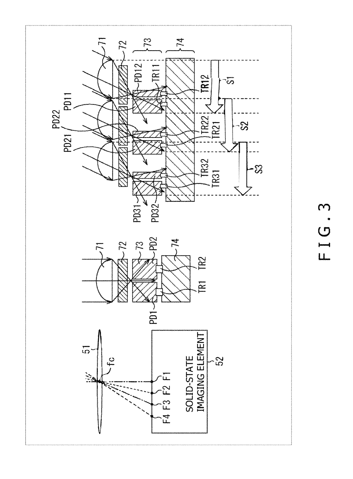
[0067]Referring to FIG. 3, a configuration example of the back surface irradiation type solid-state imaging element to which the present technology has been applied will be described below. Here, the left part of FIG. 3 is a side sectional view of a general concept of an imaging device utilizing the solid-state imaging element, the central part of FIG. 3 depicts a configuration of a side section of an on-chip lens at an image height center in the solid-state imaging element to which the present technology has been applied, and the right part of FIG. 3 depicts a configuration of a side section of an on-chip lens at a high image height of the solid-state imaging element to which the present technology has been applied.

[0068]Specifically, as depicted in the left part of FIG. 3, the imaging device to which the present technology has been applied includes a main lens 51 and a solid-state imaging element 52.

[0069]The main lens 51 focuses light from a subject onto the solid-state imaging e...

second embodiment

[0081]While an example wherein the photodiodes in the photodiode layer 73 which share the on-chip lens each include a single implant has been described hereinabove, the photodiodes may each include multiple stages of implants such as to have a shape close to a light distribution required, in accordance with the distance from an optical axis.

[0082]FIG. 5 depicts a configuration example of a back surface irradiation type solid-state imaging element wherein photodiodes each include multiple stages of implants such as to have a shape close to a light distribution required, in accordance with the distance from an optical axis. Note that the configurations having equivalent functions to those of the configurations in FIG. 3 are given the same names and denoted by the same reference signs as used above, and descriptions of them are appropriately omitted.

[0083]Note that in the following, the configuration of photodiodes PD21 and PD22 in pixels that share an on-chip lens in the center will b...

third embodiment

[0109]While an example wherein the photodiodes PD are formed by two stages of implants in forming the photodiodes PD by multiple stages of implants has been described hereinabove, the photodiodes PD may be formed by more stages of implants.

[0110]FIG. 10 depicts a configuration example of a solid-state imaging element wherein photodiodes PD21 and PD22 are formed by n stages of implants. Specifically, there is depicted that the photodiode layer 73 is formed from n stages of implants 73-1 to 73-n.

[0111]Where the photodiodes PD21 and PD22 are formed by further multiple stages of implants in this way, a shape close to a light distribution can be thereby obtained, so that focusing accuracy and sensitivity can be enhanced with higher accuracy, and color mixing can be suppressed.

[0112]It is to be noted, however, that an increase in the number of stages of implants for forming the photodiodes causes a rise in manufacturing cost, and, therefore, it is desirable to determine the number of sta...


PUM


Abstract

The present technology relates to a solid-state imaging element, an imaging device, and an electronic apparatus which enable enhancement of focusing accuracy and sensitivity and suppression of color mixing, in a high image height portion. Incident light is condensed by a main lens, and the condensed light is condensed by a plurality of on-chip lenses. The on-chip lenses are each shared by a plurality of photodiodes that receive the light condensed by the on-chip lens and that generate and accumulate electric charges corresponding to the amounts of light. The plurality of photodiodes sharing the on-chip lens are shaped, in accordance with the image height of the on-chip lens, in such a manner as to have substantially uniform light reception characteristics. The present technology is applicable to a CMOS image sensor.

Description

CROSS REFERENCE TO RELATED APPLICATIONS[0001]This application is a U.S. National Phase of International Patent Application No. PCT / JP2016 / 055794 filed on Feb. 26, 2016, which claims priority benefit of Japanese Patent Application No. JP 2015-049720 filed in the Japan Patent Office on Mar. 12, 2015. Each of the above-referenced applications is hereby incorporated herein by reference in its entirety.TECHNICAL FIELD[0002]The present technology relates to a solid-state imaging element, an imaging device and an electronic apparatus. Particularly, the present technology relates to a solid-state imaging element, an imaging device and an electronic apparatus such that it is possible to realize enhancement of focusing accuracy and sensitivity and suppression of color mixing, in a high image height portion.BACKGROUND ART[0003]In relation to digital still cameras and video cameras, there has been proposed a solid-state imaging element wherein distance detection pixels having a distance detecti...

Claims


Application Information

Patent Timeline
Patent Type & Authority Patents(United States)
IPC IPC(8): H01L31/062G01C3/06G02B7/34H01L27/146H01L27/14H04N5/374
CPCH01L27/14645G01C3/06G02B7/34H01L27/14H04N5/374H01L27/14621H01L27/14623H01L27/14627H01L27/14647H01L27/14603H04N25/76
Inventor MURASE, TAKURONOMURA, HIROTOSHI
Owner SONY CORP
Why Eureka
Try Eureka