Booster comprising a printed electronic circuit

a printed electronic circuit and booster technology, applied in the direction of printed circuit aspects, weapons, photovoltaic energy generation, etc., can solve the problems of inability to bend or easily manufacture a complex geometric shape, rigid board used for the printed circuit, and inability to make modifications to the basic circuit, etc., to achieve the effect of convenient shipping and transportation

Active Publication Date: 2019-04-23
DETNET SOUTH AFRICA (PTY) LTD
View PDF4 Cites 0 Cited by
  • Summary
  • Abstract
  • Description
  • Claims
  • Application Information

AI Technical Summary

Benefits of technology

[0017]The booster housing may be tubular and, in one form of the invention, the printed electronic circuit is printed directly onto an inner surface, or an outer surface, of the booster housing. It is preferred though to print the printed electronic circuit onto a flexible substrate, or onto two or more substrates each of which may be flexible. To provide a degree of protection for the control circuit which is included in the printed electronic circuit, it is preferred that the control circuit is carried on a substrate which, in use, is contained inside the booster housing or at a protected position on the housing. The energy harvesting module is conveniently positioned at a location at which it can be coupled, with ease, to a light emitting source. Without being restrictive the energy harvesting module would thus, normally, be on an outer side of the booster housing.
[0019]According to a further aspect of the invention the booster component is used together with a booster explosive material which is loaded into the booster housing to make up an operative booster. Preferably the design of the booster housing is such that the loading of the booster explosive material into the booster housing can readily be accomplished under non-factory conditions. This approach substantially facilitates shipping and transport of the booster component, for safety regulations which are generally applicable to explosive materials are then not required to be taken into account.

Problems solved by technology

However, once an ASIC has been committed to manufacture it is often not viable to make modifications to the basic circuit.
However, the board which is used for the printed circuit is rigid and cannot be bent nor easily manufactured in a complex geometric shape.
Additionally PCB technology is sensitive to environmental factors such as moisture.

Method used


Image

  • Booster comprising a printed electronic circuit
  • Booster comprising a printed electronic circuit
  • Booster comprising a printed electronic circuit

Examples


Embodiment Construction

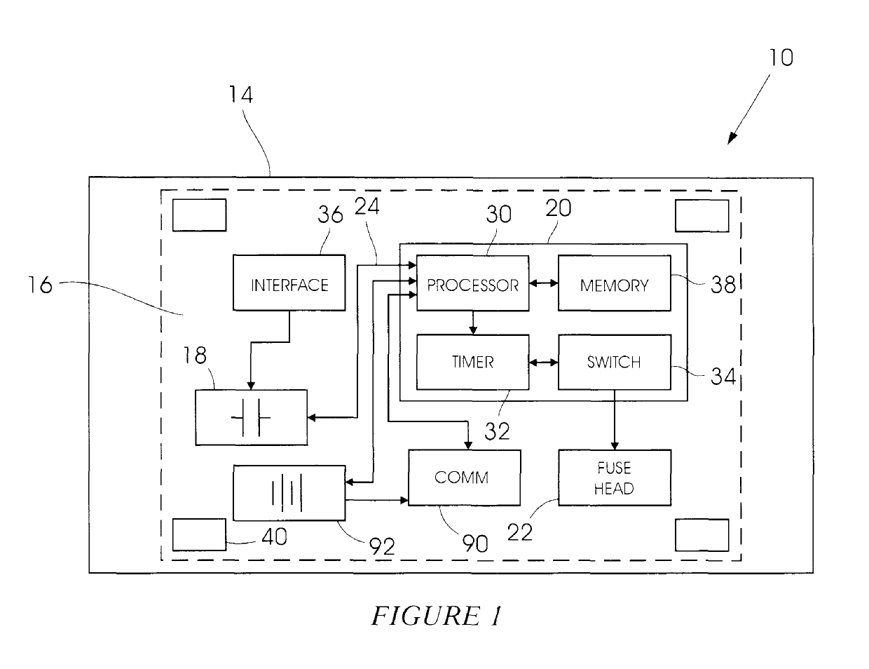
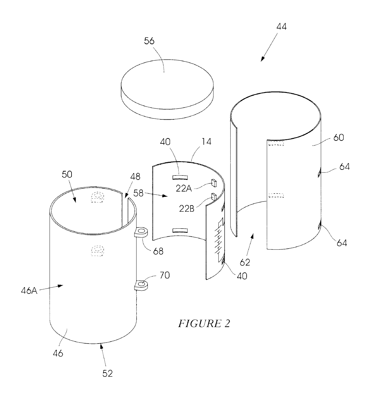
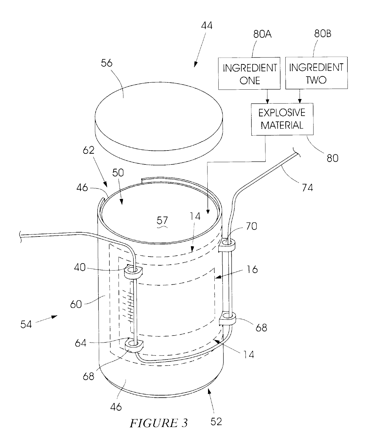
[0026]FIG. 1 of the accompanying drawings is a block diagram representation of a printed electronic circuit 10 suitable for use in a booster component according to the invention. The printed electronic circuit includes a flexible substrate 14 made from any suitable, tough, non-electrically conductive material as is known in the art. Printed on the substrate are a photovoltaic cell 16 which constitutes an energy-harvesting module, a capacitor 18, a control circuit 20 and a fuse head 22. The photovoltaic cell 16 covers a substantial area of the substrate 14. The cell preferably covers all regions of the substrate 14 not occupied by the elements 18, 20 and 22 nor by interconnecting circuit lines 24 which couple the elements to one another.

[0027]The design of the cell 16 is such that, when exposed to light, the cell 16 converts the light into electrical energy at a suitable voltage which is used to charge the capacitor 18. The capacitor 18 is a low-leakage device and is also fabricated ...


PUM


Abstract

A booster component which includes a booster housing for a booster explosive material and a printed electronic circuit which is associated with the housing and which includes a module for harvesting energy emitted by an energy source, a storage device for storing energy harvested by the module, an igniter and a circuit, powered at least by energy drawn from the storage device and responsive to a control signal for firing the igniter.

Description

BACKGROUND OF THE INVENTION[0001]This invention relates to a booster for use in an explosive system.[0002]A typical booster includes a housing which is loaded with explosive and means whereby the booster can be coupled or exposed to a detonator which, when fired, ignites the explosive.[0003]One type of detonator used with a booster is an electronic detonator. Such detonators come in different shapes and forms. Generally an electronic detonator is built on a printed circuit board making use of an application specific integrated circuit (ASIC) which is used to implement control and firing functions. Provided the ASIC is produced in an extended production run the use thereof is cost effective. However, once an ASIC has been committed to manufacture it is often not viable to make modifications to the basic circuit.[0004]As an alternative approach detonator control circuits are implemented on printed circuit boards (PCBs) using discrete components. A product produced in this way is robus...

Claims


Application Information

Patent Timeline
Patent Type & Authority Patents(United States)
IPC IPC(8): F42D1/05F42B3/12H05K1/02H05K1/16H05K3/00
CPCF42D1/05F42B3/121H05K1/0284H05K1/16H05K3/0058H05K2201/056H05K2201/09063H05K2201/0999Y02E10/50Y02E70/30
Inventor MULLER, ELMARVENTER, FRANCOIS
Owner DETNET SOUTH AFRICA (PTY) LTD
Why Eureka
Try Eureka