Semiconductor module

a technology of semiconductor modules and semiconductors, applied in the direction of semiconductor devices, semiconductor/solid-state device details, electrical apparatus, etc., can solve the problems of reducing the safe operating area affecting the safety of short-circuit semiconductor modules, and slow switching of certain igbts, etc., to achieve the effect of increasing the current rating

Active Publication Date: 2019-04-30
HITACHI ENERGY LTD
View PDF16 Cites 0 Cited by
  • Summary
  • Abstract
  • Description
  • Claims
  • Application Information

AI Technical Summary

Benefits of technology

[0008]It is an objective of the invention to provide a semiconductor module with good thermal behavior and well balanced electro-magnetic coupling behavior.
[0018]The semiconductor switch chip (and particular its emitter electrode) may be directly connected via one or more bond wires with the protruding area. In such a way, an additional emitter current path between the emitter conductor and the semiconductor switch chip is formed, which may inductively couple with a bond wire interconnecting the gate electrode of the semiconductor switch chip and the gate conductor. This inductive coupling may lower the voltage drop at the gate of the semiconductor switch chip. In such way, the switching behaviour and / or the switching speed of the semiconductor switch may be set and / or adapted with the additional emitter current path.
[0025]According to an embodiment of the invention, a gate electrode of the semiconductor switch chip is connected via a bond wire with a bridging conductor on the substrate plate, which is at least partially surrounded by the protruding area of the emitter conductor and which is connected via a bond wire with the gate conductor. The bridging conductor may be seen as a conductor island, which may be provided by a metallization layer on the substrate of the substrate plate. For example, a part of the metallization layer providing the protruding area may be disconnected from the protruding area and used as bridging conductor. With the bridging conductor, the direction of a bond wire connecting the bridging conductor and the gate electrode of the semiconductor switch chip with respect to a bond wire connecting the protruding area of the emitter conductor with the emitter electrode of the first semiconductor switch chip, may be adjusted more easily. Thus, the inductive coupling between the gate current path and the additional emitter current path may be adjusted more easily.
[0027]According to an embodiment of the invention, the gate electrode of the semiconductor switch chip is provided at a gate electrode side of the semiconductor switch chip and the semiconductor switch chip is positioned such that its gate electrode side points towards diode chip, for example to a side of the semiconductor module with the emitter conductor. The gate electrode (which may be much smaller than the emitter electrode) may be provided at an edge of the semiconductor switch chip. The semiconductor switch chip may be positioned in such a way, that this edge is at the side of the semiconductor switch chip, which is nearer to the gate electrode as the other side. In such a way, the corresponding gate current path may be shortened.
[0034]The parallelization of the semiconductor switch chips and the rows of chips, respectively, may advantageously provide a higher current rating than a row alone. All chips may be bonded to the collector conductor, which also may provide a collector connection of the semiconductor module. With the above described arrangement, no semiconductor switch chip has to be placed directly besides another semiconductor switch chip. This may provide a better thermal behavior of the semiconductor module. On the other hand, due to the additional emitter current path, the switching behaviour of the first and second semiconductor switch chips may be adapted to each other.

Problems solved by technology

This distortion may lead to certain IGBTs switching slower compared to others.
Such a current imbalance may be undesired and may especially reduce the short circuit safe operating area of the semiconductor module.

Method used


Image

  • Semiconductor module
  • Semiconductor module
  • Semiconductor module

Examples


Embodiment Construction

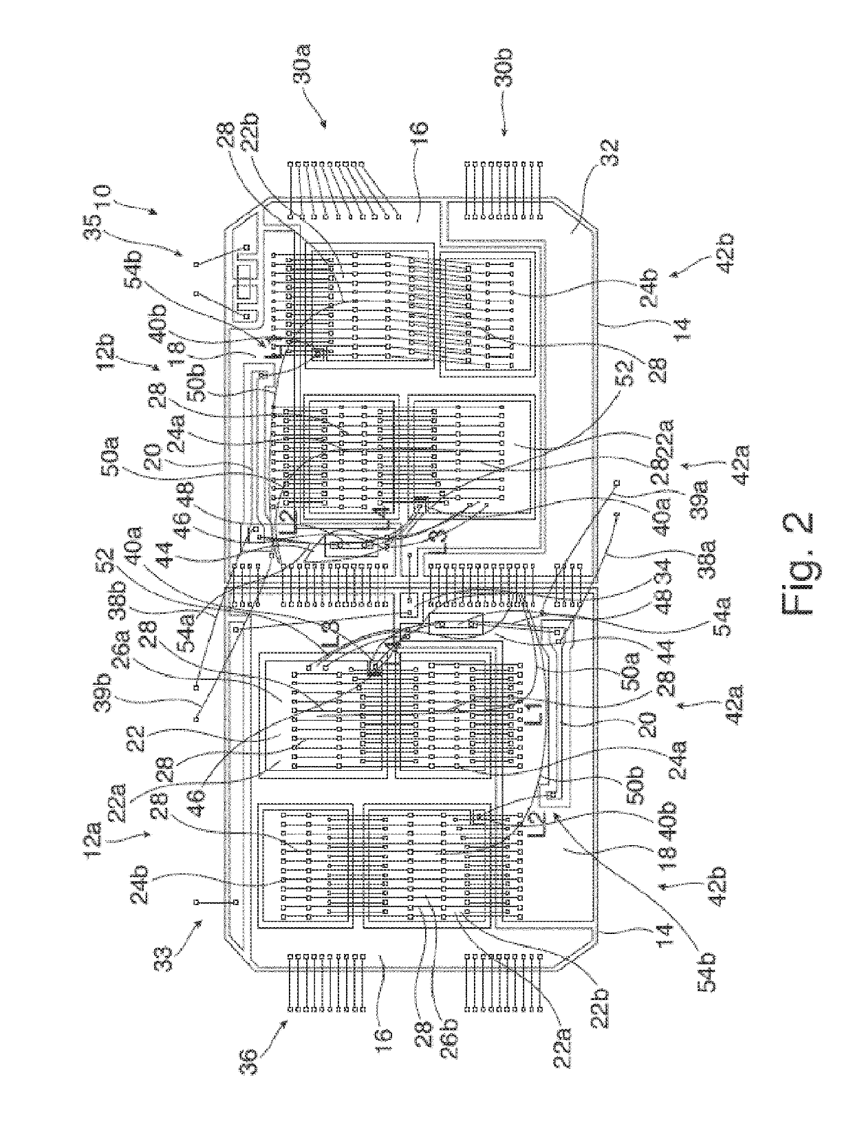
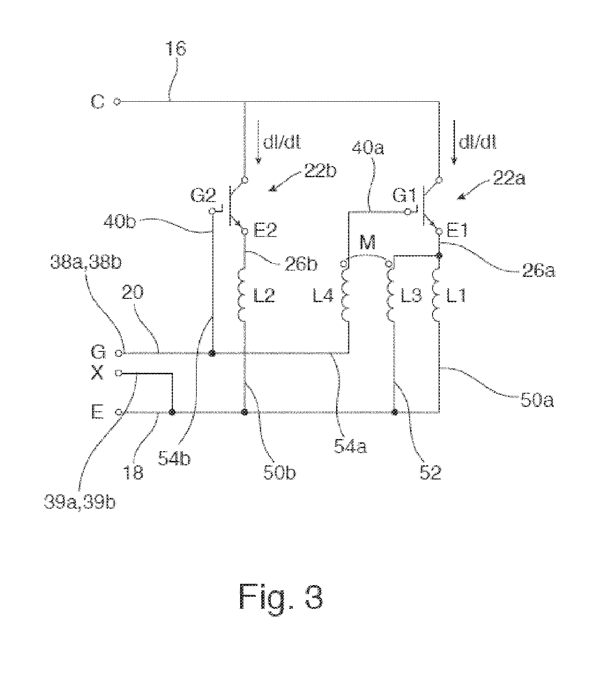
[0006]A symmetric arrangement of chips may result in a bad temperature distribution within the semiconductor module. The semiconductor switch chips as well as the diode chips are all concentrated on specific areas on the substrate plate.

[0007]When the chips are distributed more homogeneously over the semiconductor module, this may result in a better temperature distribution. However, in this case, some semiconductor switches may have a longer emitter current path than others. Different inductive voltage drops in these paths may cause current imbalances within the semiconductor module.

[0008]It is an objective of the invention to provide a semiconductor module with good thermal behavior and well balanced electro-magnetic coupling behavior.

[0009]This objective is achieved by the subject-matter of the independent claims. Further exemplary embodiments are evident from the dependent claims and the following description.

[0010]The invention relates to a semiconductor module, which, for exam...


PUM


Abstract

A semiconductor module, comprises a substrate plate; a semiconductor switch chip and a diode chip attached to a collector conductor on the substrate plate, wherein the diode chip is electrically connected antiparallel to the semiconductor switch chip; wherein the semiconductor switch chip is electrically connected via bond wires to an emitter conductor on the substrate plate providing a first emitter current path, which emitter conductor is arranged oppositely to the semiconductor switch chip with respect to the diode chip; wherein a gate electrode of the semiconductor switch chip is electrically connected via a bond wire to a gate conductor on the substrate plate providing a gate current path, which gate conductor is arranged oppositely to the semiconductor switch chip with respect to the diode chip; and wherein a protruding area of the emitter conductor runs besides the diode chip towards the first semiconductor switch chip and the first semiconductor switch chip is directly connected via a bond wire with the protruding area providing an additional emitter current path running at least partially along the gate current path. The semiconductor switch chip is a first semiconductor switch chip and the diode chip is a first diode chip, which are arranged in a first row. The semiconductor module comprises further a second row of a second semiconductor switch chip and a second diode chip attached to the collector conductor, wherein the diode chip of each row is electrically connected antiparallel to the semiconductor switch chip of the same row and the first and second rows are electrically connected in parallel. The first semiconductor switch chip is arranged besides the second diode chip and the second semiconductor chip is arranged besides the first diode chip.

Description

FIELD OF THE INVENTION[0001]The invention relates to the field of packaging several semiconductor chips into a module. In particular, the invention relates to a semiconductor module.BACKGROUND OF THE INVENTION[0002]In IGBT power semiconductor modules, typically several IGBT chips and free-wheeling diode chips are connected in parallel to reach the desired module current rating. The gate signal for switching the IGBTs is fed from the outer gate terminals of the semiconductor module to each IGBT chip. In this gate current path, the signal may be distorted during turn-on of the IGBTs. This distortion may lead to certain IGBTs switching slower compared to others. Such a current imbalance may be undesired and may especially reduce the short circuit safe operating area of the semiconductor module.[0003]To produce a low distortion, it is possible to arrange the semiconductor switches side by side in a symmetric way such that the emitter current paths and the gate current paths, respectivel...

Claims


Application Information

Patent Timeline
Patent Type & Authority Patents(United States)
IPC IPC(8): H01L25/18H01L25/07H01L23/00H01L23/498H01L23/538
CPCH01L25/18H01L23/49811H01L23/49838H01L23/5381H01L24/48H01L24/49H01L25/072H01L2924/30107H01L2924/19107H01L2924/15787H01L2924/13091H01L2924/13055H01L2924/1203H01L2924/10161H01L24/05H01L24/06H01L2224/0603H01L2224/4846H01L2224/48137H01L2224/48139H01L2224/48227H01L2224/49111H01L2224/49175H01L2224/49431H01L2224/49433H01L2924/00014H01L2224/45099H01L2224/05599H01L2924/00012
Inventor HARTMANN, SAMUELSCHLAPBACH, ULRICH
Owner HITACHI ENERGY LTD
Why Eureka
Try Eureka