Cu—Ga binary alloy sputtering target and method of producing the same

a technology of binary alloys and sputtering targets, applied in the direction of vacuum evaporation coatings, coatings, electric discharge tubes, etc., can solve the problems of high density sputtering targets, high bending strength, and increased workability, so as to achieve high bending strength, easy surface machining, and high density

Active Publication Date: 2019-05-07
MITSUBISHI MATERIALS CORP
View PDF51 Cites 0 Cited by
  • Summary
  • Abstract
  • Description
  • Claims
  • Application Information

AI Technical Summary

Benefits of technology

[0033]According to the present invention, the technical effects described below can be obtained.
[0034]According to the Cu—Ga binary alloy sputtering target and the method of producing the target related to the present invention, cracking or fracturing does not occur during cutting and the target has high density and high bending strength, since the target has the coexistence microstructure, in which the low-Ga-containing Cu—Ga binary alloy phase is surrounded by the high-Ga-containing Cu—Ga binary alloy phase. Therefore, surface machining can be performed easily by cutting; the machining speed of the sputtering target is fast; and the target with a complex shape can be machined easily, in the sputtering target related to the present invention. In addition, the target is resistant to thermal shock during sputtering since it has high density and high bending strength. Thus, cracking of the target or the like can be suppressed.
[0035]In addition, sodium (Na) can be added to the light-absorbing layer to improve the efficiency of electric power generation of the layer by utilizing this Cu—Ga binary alloy sputtering target for sputtering film deposition during formation of the light-absorbing layer made of the Cu—In—Ga—Se quaternary alloy film of a solar cell in the case where the Cu—Ga binary alloy sputtering target related to the present invention includes Na component.

Problems solved by technology

Conventionally, in the CuGa sputtering target with high density and high Ga content used for formation of the light-absorbing layer, particularly in the case where Ga content exceeds 28 atomic %, the highly-densified sputtering target becomes very hard and inductile since the deposition ratio of the brittle γ phase with poor workability is increased.
Particularly, in the case where it is a casting by melting and casting, cutting work is difficult since cracking or fracturing occur during surface machining by cutting.
Because of this, machining speed of the target is slow, and machining of the target with a complex shape is very difficult.

Method used


Image

  • Cu—Ga binary alloy sputtering target and method of producing the same
  • Cu—Ga binary alloy sputtering target and method of producing the same
  • Cu—Ga binary alloy sputtering target and method of producing the same

Examples


first embodiment

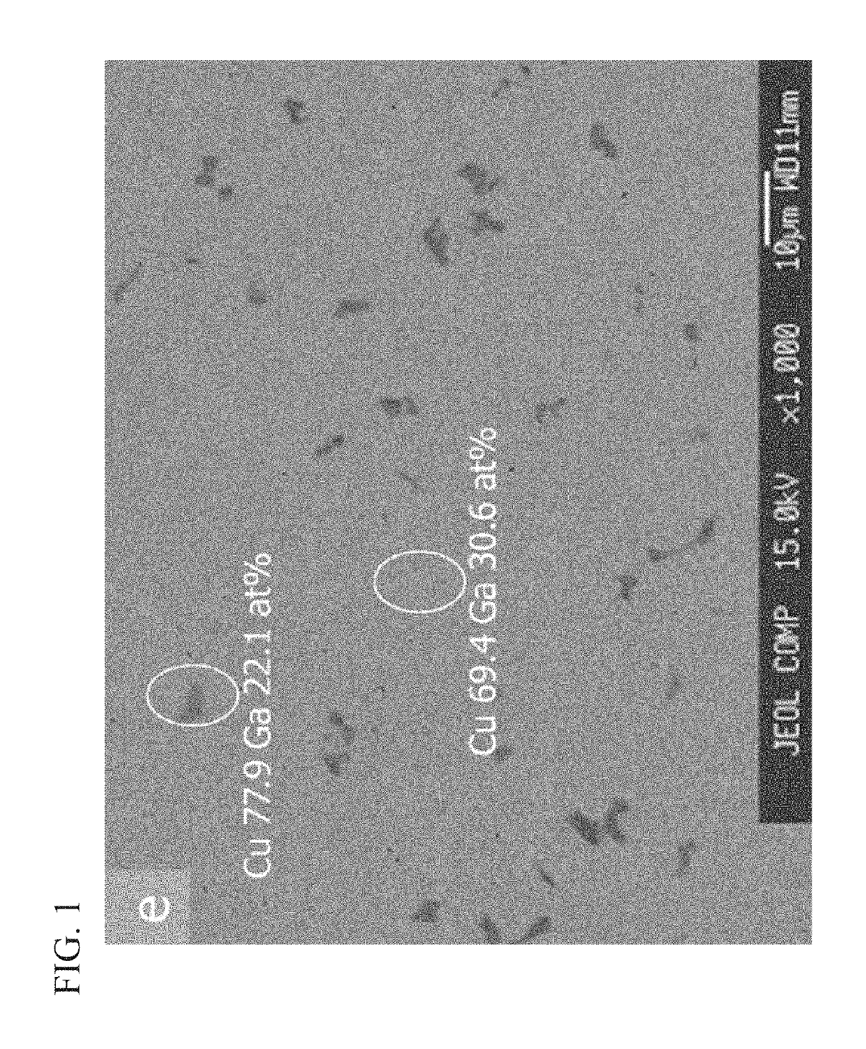
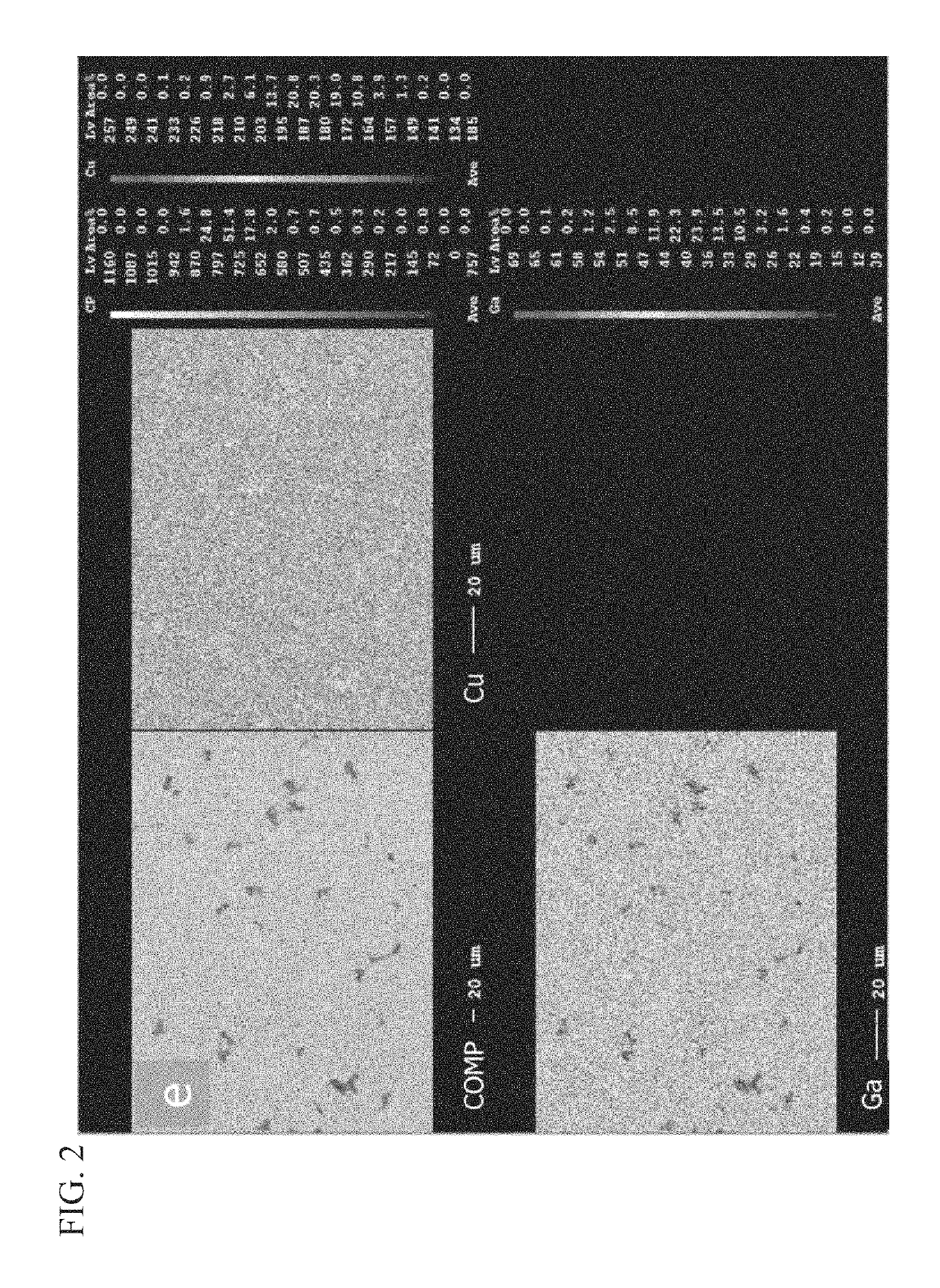
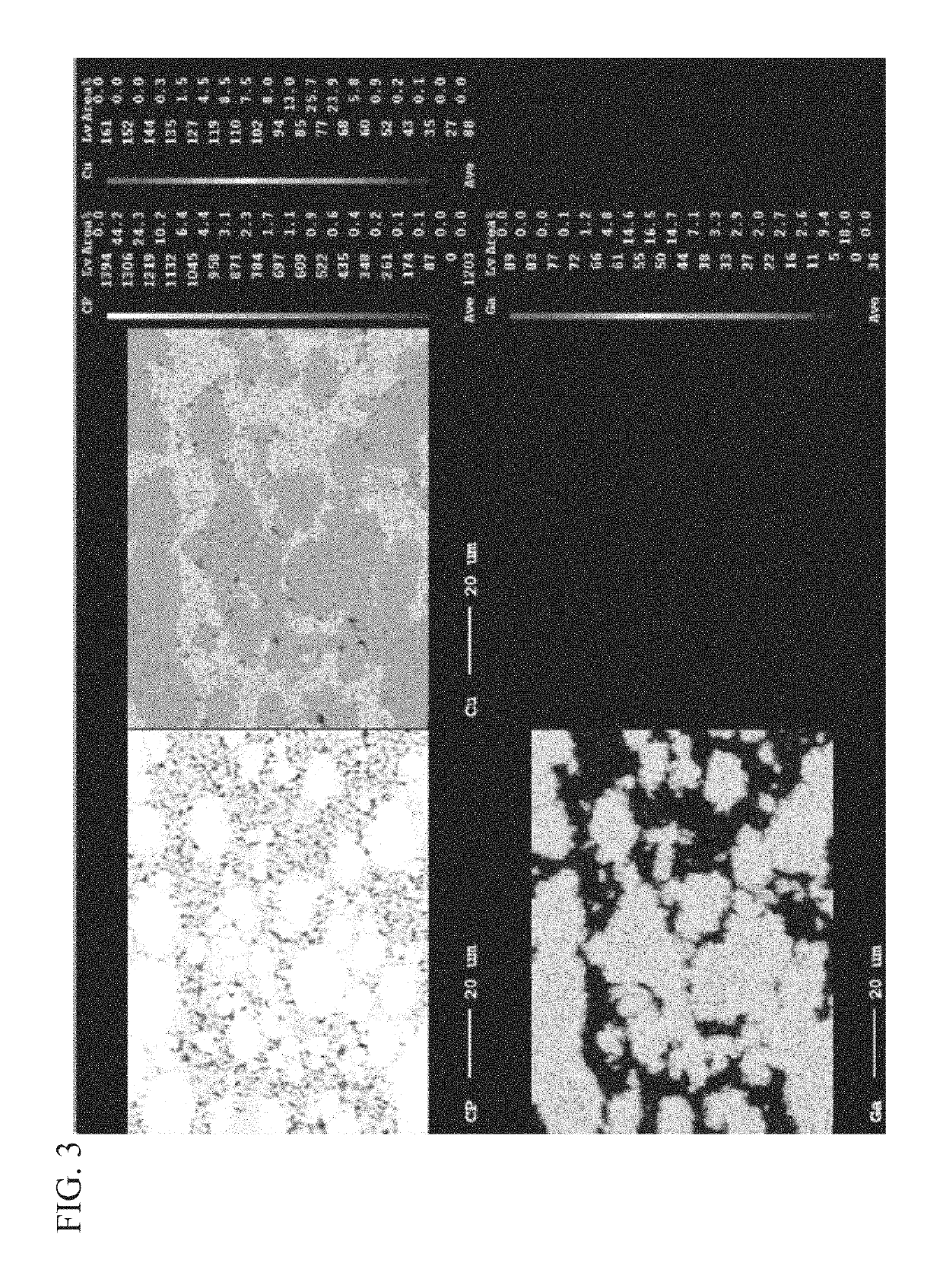
[0040]The Cu—Ga binary alloy sputtering target of the first embodiment has a composition including 28 to 35 atomic % of Ga and the Cu balance and inevitable impurities. In addition, the sputtering target has a coexistence microstructure in which the low-Ga-containing Cu—Ga binary alloy phase, which includes 26 atomic % or less of Ga and the Cu balance and inevitable impurities, is surrounded by the high-Ga-containing Cu—Ga binary alloy phase, which includes 28 atomic % or more of Ga.

[0041]A preferable lower limit of the Ga content in the low-Ga-containing binary alloy phase is 15 atomic %. A preferable upper limit of the Ga content in the high-Ga-containing Cu—Ga binary alloy phase is 40 atomic %.

[0042]The coexistence microstructure can be observed by element mapping images of Cu and Ga obtained by the electron microprobe (EPMA) as shown in FIGS. 1 and 2, for example.

[0043]In the Cu—Ga binary alloy sputtering targets of the specific examples of the present invention shown in FIGS. 1...

second embodiment

[0075]As explained above, the sputtering target has the coexistence microstructure, in which the low-Ga-containing Cu—Ga binary alloy phase is surrounded by the high-Ga-containing Cu—Ga binary alloy phase, in the Cu—Ga binary alloy sputtering target of the first embodiment of the present invention. In the Cu—Ga binary alloy sputtering target of the second embodiment of the present invention, Na or Na compound is added to the Cu—Ga binary alloy sputtering target of the first embodiment with the coexistence microstructure.

Example (Ex.)

[0076]As raw material powders used for examples of the present invention, the high-Ga-containing Cu—Ga binary alloy powder and low-Ga-containing Cu—Ga binary alloy powder prepared as in the first embodiment of the present invention can be used. The high-Ga-containing Cu—Ga binary alloy powder and low-Ga-containing Cu—Ga binary alloy powder having the compositions and the average sizes shown in Table 3 below were prepared. The Ga contents are shown in the...


PUM

PropertyMeasurementUnit
grain sizeaaaaaaaaaa

Abstract

A Cu—Ga binary alloy sputtering target having excellent mechanical workability, high density, and high bending strength, and a method of producing the sputtering target are provided. The sputtering target has a composition including 28 to 35 atomic % of Ga and the balance made of Cu and inevitable impurities. In addition, the sputtering target has a coexistence microstructure in which a low-Ga-containing Cu—Ga binary alloy phase is surrounded by a high-Ga-containing Cu—Ga binary alloy phase. The low-Ga-containing Cu—Ga binary alloy phase includes 26 atomic % or less of Ga and a balance made of Cu. The high-Ga-containing Cu—Ga binary alloy phase includes 28 atomic % or more of Ga.

Description

FIELD OF THE INVENTION[0001]The present invention relates to a Cu—Ga binary alloy sputtering target, which is used for forming a film of Cu—In—Ga—Se quaternary alloy as a light-absorbing layer of a solar cell, for example, and a method of producing the Cu—Ga binary alloy sputtering target.[0002]Priority is claimed on Japanese Patent Application No. 2012-229469, filed Oct. 17, 2012, and Japanese Patent Application No. 2013-208191, filed Oct. 3, 2013, the contents of which are incorporated herein by reference.BACKGROUND OF THE INVENTION[0003]The Cu—Ga sputtering target has been the essential material for producing a solar cell with the Cu—In—Ga—Se quaternary alloy film (CIGS film) as its light-absorbing layer by so-called “selenization method.” The selenization method is a method of forming a film of CuInGaSe compound, for example, by heating a laminated film, in which CuGa is sputtered at about 500 nm and an In film is sputtered on the sputtered CuGa at the thickness of about 500 nm,...

Claims


Application Information

Patent Timeline
Patent Type & Authority Patents(United States)
IPC IPC(8): B22F3/14C22C28/00C22C1/04C22C9/00B22F3/24C23C14/34B22F3/15B22F3/10H01J37/34
CPCH01J37/3426B22F3/10B22F3/14B22F3/15C22C1/0425C22C9/00C22C28/00C23C14/3414B22F3/24B22F2003/247
Inventor UMEMOTO, KEITAZHANG, SHOUBIN
Owner MITSUBISHI MATERIALS CORP
Why Eureka
Try Eureka