Plasma generation apparatus, CVD apparatus, and plasma-treated particle generation apparatus
a technology of plasma generation apparatus and cvd, which is applied in the direction of plasma technique, chemical vapor deposition coating, coating, etc., can solve the problems of deterioration in the performance of a semiconductor function, long time required for film formation, and difficulty in considerably improving the time period for film formation, so as to prevent the occurrence of inner surface corrosion, prevent the occurrence of electrode corrosion, and reduce the time of film formation.
- Summary
- Abstract
- Description
- Claims
- Application Information
AI Technical Summary
Benefits of technology
Problems solved by technology
Method used
Image
Examples
embodiment 1
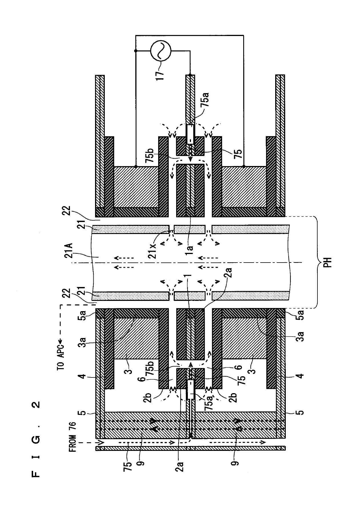
[0158]The insulating tube 21 shown in FIG. 4 may be omitted, too. In such a case, it can be considered that portions of the insulating plate 4, the dielectrics 2a, 2b, and the insulators 1a, 3a, 5a facing the continuous through hole described in the embodiment 1 constitute a member that can be regarded as the insulating tube 21. Additionally, it can be considered that an end portion of the discharge space 6 facing the continuous through hole serves as the ejection hole 21x.
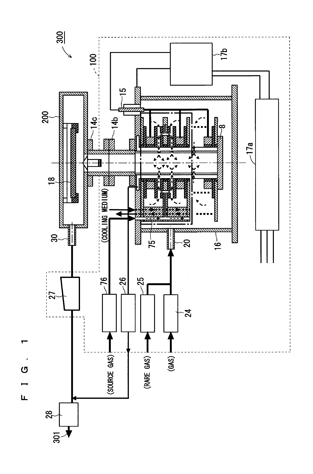
[0159]As shown in FIG. 4, the plasma-treated particle generation apparatus 400 includes a plasma generation apparatus 100, a processed material collection flange 250, and an exhaust gas decomposition processor 28.
[0160]A configuration of the plasma generation apparatus 100 according to the present invention will be described.
[0161]Most of the configuration of the plasma generation apparatus 100 according to the embodiment 2, including the configuration (the configuration shown in FIG. 2) of the electrode cell, is...
embodiment 3
[0266]Here, an example case in which an ozone gas is adopted as the source gas containing the active gas will be described as an example of an
[0267]In a process for forming an oxide film on a surface of a semiconductor wafer in the CVD apparatus 300, an oxygen gas or an ozone gas is used as the source gas. In the CVD chamber 200, the surface of the semiconductor wafer is exposed to activated oxygen atoms, so that film formation is performed. In the formation of such an oxide film, it has been demanded that a time period for the film formation process be shortened, that insulating properties be improved, and that the processing performance be improved. An ozone gas, from which activated atoms are easily obtained, is desired as the supplied source gas. Furthermore, an increase in the concentration and flow rate of the ozone gas is also desired.
[0268]However, the concentration of ozone obtained from an ozone generation apparatus is limited because of the principle of generation. The oz...
PUM
| Property | Measurement | Unit |
|---|---|---|
| energy density | aaaaa | aaaaa |
| pressure | aaaaa | aaaaa |
| temperature | aaaaa | aaaaa |
Abstract
Description
Claims
Application Information


