Semiconductor devices, semiconductor packages, and methods of manufacturing the semiconductor devices

a technology of semiconductor chips and semiconductor packaging, which is applied in the direction of semiconductor devices, semiconductor/solid-state device details, electrical apparatus, etc., can solve the problems of deterioration of reliability and electrical interconnection of such stacked semiconductor chips, and achieve high joint reliability

Active Publication Date: 2019-06-18
SAMSUNG ELECTRONICS CO LTD
View PDF20 Cites 3 Cited by
  • Summary
  • Abstract
  • Description
  • Claims
  • Application Information

AI Technical Summary

Benefits of technology

[0004]The inventive concepts provide a semiconductor device including a pad structure having high joint reliability, a semiconductor package, and methods of manufacturing the semiconductor device and the semiconductor package.

Problems solved by technology

However, complications may arise in electrical interconnection of such stacked semiconductor chips, for instance, due to step differences in interconnecting pad structures.
In particular examples, trapping of non-conductive materials and / or forming of intermetallic compounds (IMC) may occur due to such step differences, which may degrade reliability.

Method used


Image

  • Semiconductor devices, semiconductor packages, and methods of manufacturing the semiconductor devices
  • Semiconductor devices, semiconductor packages, and methods of manufacturing the semiconductor devices
  • Semiconductor devices, semiconductor packages, and methods of manufacturing the semiconductor devices

Examples


Embodiment Construction

[0018]The inventive concepts will now be described more fully with reference to the accompanying drawings, in which embodiments of the inventive concepts are shown.

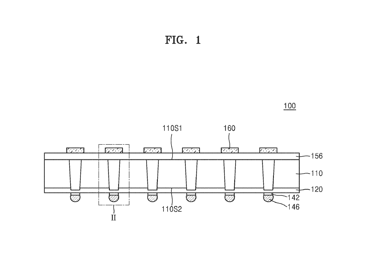
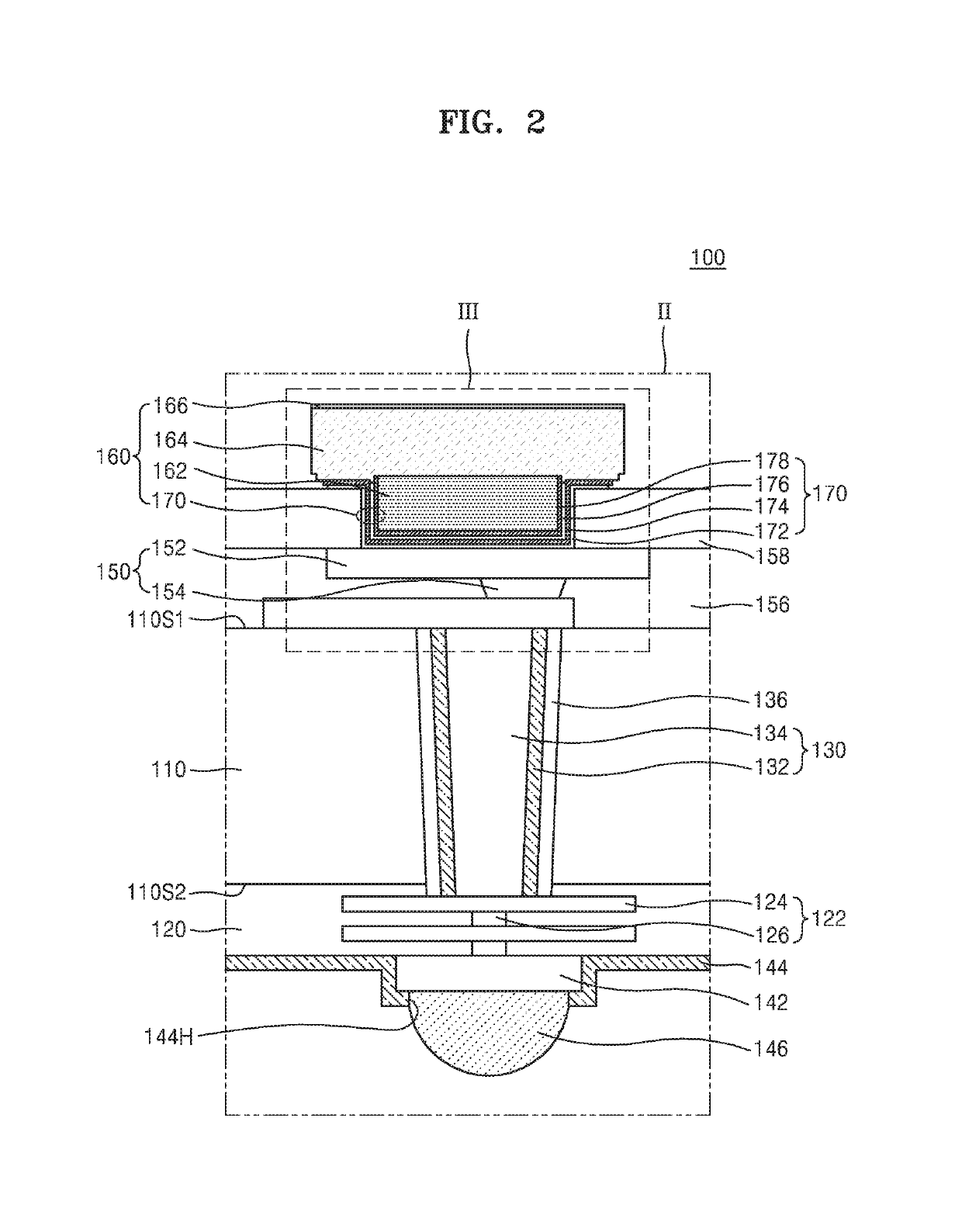
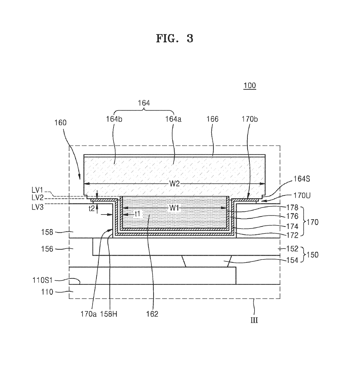
[0019]FIG. 1 is a cross-sectional view of a semiconductor device 100 according to some embodiments. FIG. 2 is an enlarged cross-sectional view of a portion II of FIG. 1. FIG. 3 is an enlarged cross-sectional view of a portion III of FIG. 2.

[0020]Referring to FIGS. 1 to 3, a substrate 110 may include a first surface 110S1 and a second surface 110S2, which is a reverse side of the first surface 110S1. Although the terms first, second, etc. may be used herein to describe various elements, these terms are only used to distinguish one element from another element, and these elements should not be limited by these terms. Thus, a first element could be termed a second element without departing from the scope of the present inventive concepts. The substrate 110 may include, for example, silicon (Si). The substrate 110 may include...


PUM


Abstract

A semiconductor device includes a conductive component on a substrate, a passivation layer on the substrate and including an opening that exposes at least a portion of the conductive component, and a pad structure in the opening and located on the passivation layer, the pad structure being electrically connected to the conductive component. The pad structure includes a lower conductive layer conformally extending on an inner sidewall of the opening, the lower conductive layer including a conductive barrier layer, a first seed layer, an etch stop layer, and a second seed layer that are sequentially stacked, a first pad layer on the lower conductive layer and at least partially filling the opening, and a second pad layer on the first pad layer and being in contact with a peripheral portion of the lower conductive layer located on the top surface of the passivation layer

Description

CROSS-REFERENCE TO RELATED APPLICATION[0001]This application claims the benefit of Korean Patent Application No. 10-2017-0093692, filed on Jul. 24, 2017, in the Korean Intellectual Property Office, the disclosure of which is incorporated herein in its entirety by reference.BACKGROUND[0002]The inventive concepts relate to semiconductor devices, semiconductor packages, and methods of manufacturing the semiconductor devices, and more particularly, to semiconductor devices including pad structures and methods of manufacturing semiconductor devices.[0003]In accordance with the rapid development of the electronics industry and user demand, electronic devices are being manufactured to be smaller in size and weight, and semiconductor packages used for the electronic devices have needed not only to be small and lightweight, but also to have high performance and high capacity. With the growing tendency toward smaller and lighter semiconductor packages, research into semiconductor packages inc...

Claims


Application Information

Patent Timeline
Patent Type & Authority Patents(United States)
IPC IPC(8): H01L23/48H01L25/065H01L23/31H01L23/00
CPCH01L24/05H01L23/3171H01L23/481H01L24/03H01L24/13H01L24/16H01L25/0657H01L2224/05582H01L2224/05624H01L2224/05639H01L2224/05644H01L2224/05655H01L2224/05669H01L2224/05684H01L2224/13024H01L2224/13025H01L2224/16145H01L2224/16227H01L2225/06513H01L2225/06517H01L2225/06541H01L2225/06586H01L2924/04941H01L2924/04953H01L2224/03416H01L2224/03418H01L2224/03452H01L2224/03462H01L2224/03464H01L2224/03614H01L2224/03916H01L2224/0401H01L2224/0508H01L2224/05017H01L2224/05022H01L2224/05024H01L2224/05124H01L2224/05144H01L2224/05147H01L2224/05164H01L2224/05166H01L2224/05169H01L2224/05171H01L2224/05181H01L2224/05184H01L2224/05557H01L2224/05562H01L2224/05568H01L21/4814H01L23/488H01L23/3128H01L23/3135H01L24/17H01L24/32H01L24/73H01L24/81H01L24/92H01L25/18H01L2224/05564H01L2224/05567H01L2224/05647H01L2224/06181H01L2224/13022H01L2224/16148H01L2224/17181H01L2224/32145H01L2224/32225H01L2224/73204H01L2224/81203H01L2224/81815H01L2224/92125H01L2924/15311H01L2224/03831H01L2224/05085H01L2224/0362H01L2224/05016H01L2224/05155H01L2224/05558H01L2224/13082H01L2224/13109H01L2224/13111H01L2224/13113H01L2224/13116H01L2224/13118H01L2224/1312H01L2224/13139H01L2224/13144H01L2224/13147H01L2224/13155H01L2224/13164H01L2224/13169H01L2224/8181H01L2924/01029H01L2924/01082H01L2924/01047H01L2924/01079H01L2924/01083H01L2924/0103H01L2924/013H01L2924/00014H01L2924/00H01L2224/16225H01L23/485H01L23/5384H01L23/538
Inventor CHOI, JU-ILMOON, KWANG-JINSEO, JU-BINLIM, DONG-CHANFUJISAKI, ATSUSHILEE, HO-JIN
Owner SAMSUNG ELECTRONICS CO LTD
Why Eureka
Try Eureka