Ceramic electronic device

a ceramic electronic device and ceramic technology, applied in the direction of fixed capacitor details, stacked capacitors, fixed capacitors, etc., can solve the problem of stress generation in the interface between the baked electrode and the surface, and achieve the effect of high joint reliability

Pending Publication Date: 2022-09-08
TDK CORPARATION
View PDF11 Cites 0 Cited by
  • Summary
  • Abstract
  • Description
  • Claims
  • Application Information

AI Technical Summary

Benefits of technology

[0005]The present invention has been achieved under such circumstances. It is an object of the present invention to provide a ceramic electronic device having a high joint reliability between an element body and an external electrode.

Problems solved by technology

When a load, such as thermal shock, is applied to the ceramic electronic device, however, stress is generated in the interface between the baked electrode and the surface of the element body, and the baked electrode may peel off from the surface of the element body.

Method used


Image

  • Ceramic electronic device
  • Ceramic electronic device

Examples


examples

[0093]Hereinafter, the present invention is explained in more detail with examples of the present invention, but the present invention is not limited to the examples.

experiment 1

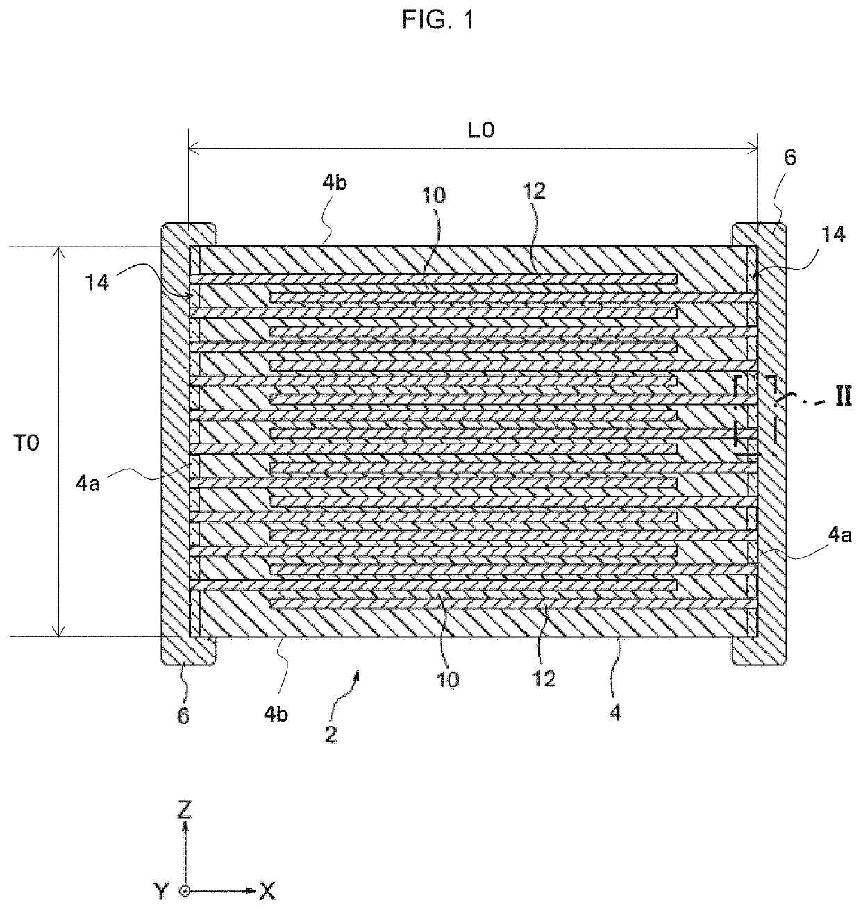
[0094]In Experiment 1, multilayer ceramic capacitors 2 according to Examples 1-3 were manufactured in the following manner. First, a dielectric paste and an internal-electrode paste were prepared, and green chips were manufactured by a sheet method using the pastes. At this time, as a dielectric raw material to be a main component of ceramic layers 10, barium titanate (BT) was used in Example 1 and Example 2, and barium titanate calcium (BCT) was used in Example 3. In each Example, MgCO3, MnCO3, Y2O3, SiO2, and the like were added as sub-components of the ceramic layers 10, and the main component of internal electrode layers 12 was Ni.

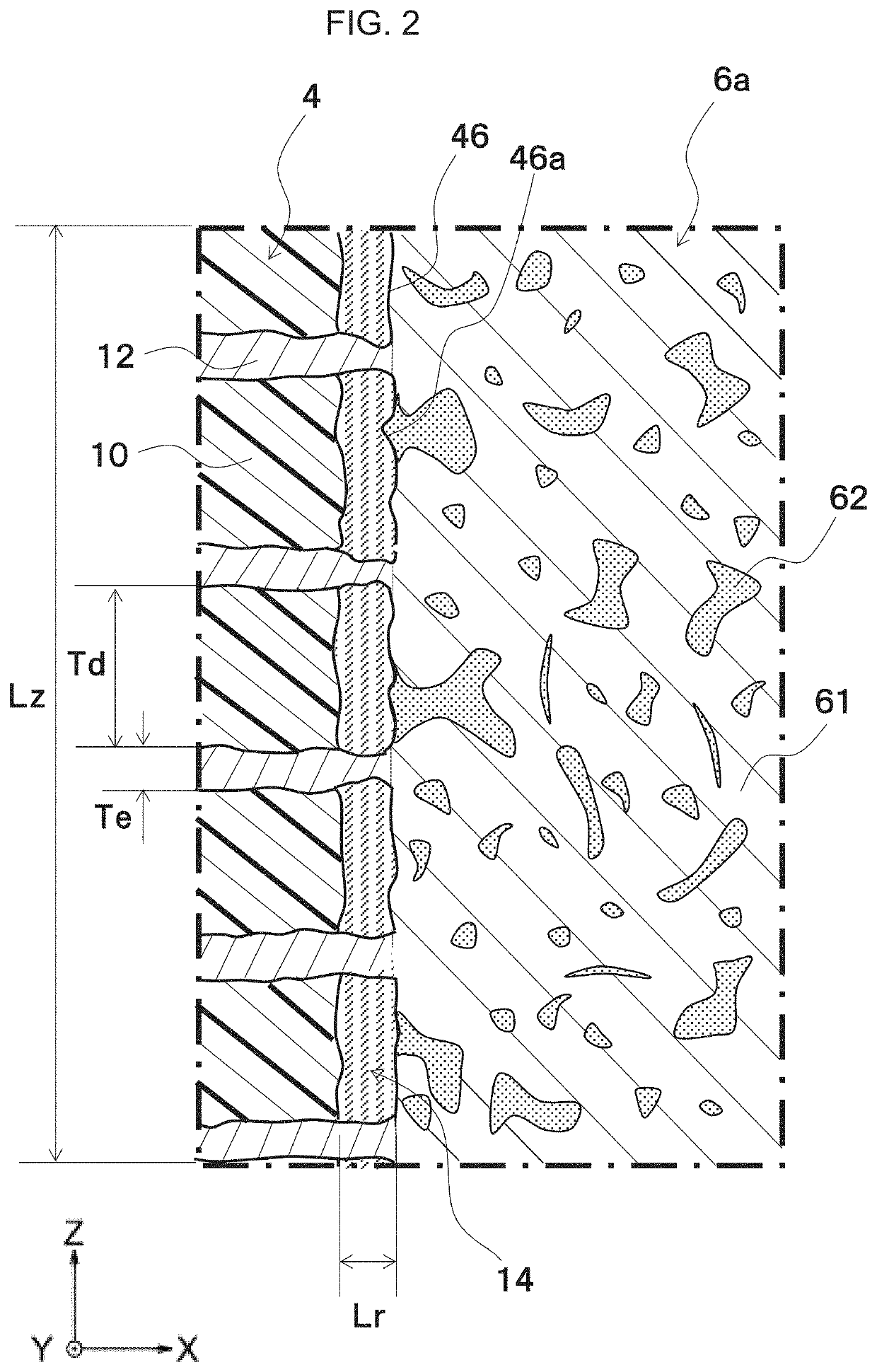
[0095]Next, the green chips obtained above were subjected to a binder removal treatment with the conditions mentioned in the embodiment, and a boundary-layer paste was applied to the outer surfaces (end surfaces) of the green chips by a dipping method and dried. As a main component of the boundary layer 14, a BaZnSiO4 powder was added to the boundary-l...

experiment 2

[0111]In Experiment 2, the capacitor samples according to Examples 4-6 were manufactured by changing the method of forming the boundary layers 14. The method of forming the boundary layers 14 in each Example is explained below.


PUM

PropertyMeasurementUnit
thicknessaaaaaaaaaa
thicknessaaaaaaaaaa
thicknessaaaaaaaaaa

Abstract

A ceramic electronic device includes an element body and an external electrode. The element body includes a ceramic layer and an internal electrode layer. The external electrode is formed on an end surface of the element body and electrically connected to a part of the internal electrode layer. The ceramic layer includes a perovskite compound represented by ABO3 as a main component. The external electrode includes a conductor and a glass frit diffused in the conductor. The glass frit includes B, Si, Ba, and Zn. A boundary layer is present at an end of the ceramic layer in contact with the external electrode on the end surface of the element body and comprises an oxide including Ba, Zn, and Si.

Description

BACKGROUND OF THE INVENTION[0001]The present invention relates to a ceramic electronic device including an external electrode.[0002]As shown in Patent Document 1, a ceramic electronic device including an element body containing a ceramic component and external electrodes formed on an outer surface of the element body is known. Baked electrodes are widely used as external electrodes for ceramic electronic devices, and the baked electrodes can be formed by applying a conductive paste containing conductor powder and glass frit to the surface of the element body and baking it. The baked electrodes can have a higher joint strength as compared with when a plating electrode or a resin electrode is directly formed on the surface of the element body.[0003]When a load, such as thermal shock, is applied to the ceramic electronic device, however, stress is generated in the interface between the baked electrode and the surface of the element body, and the baked electrode may peel off from the su...

Claims


Application Information

Patent Timeline
Patent Type & Authority Applications(United States)
IPC IPC(8): H01G4/232H01G4/30H01G4/12
CPCH01G4/2325H01G4/30H01G4/1227H01G4/1209H01G4/008H01G4/232H01G4/002H01G4/012
Inventor IGUCHI, TOSHIHIROSUEDA, YUICHIRONAMIKI, RYOTA
Owner TDK CORPARATION
Why Eureka
Try Eureka