Electronic component mounting method, and circuit substrate and circuit substrate unit used in the method

a technology of electronic components and mounting methods, which is applied in the direction of sustainable manufacturing/processing, final product manufacturing, cooking vessels, etc., can solve the problems of lowering joint strength, high cost, complex production process, etc., and achieves high joint reliability, good product quality, and reliable reinforcement

Inactive Publication Date: 2007-07-19
PANASONIC CORP
View PDF9 Cites 11 Cited by
  • Summary
  • Abstract
  • Description
  • Claims
  • Application Information

AI Technical Summary

Benefits of technology

[0048] With this design, the circuit substrate units are produced by the above-described electronic component mounting method with high joint reliability between the components and substrate and with good productivity. Even when the components are densely mounted on the substrate and closely spaced from one another, their joints are reinforced reliably and with good productivity, due to the reinforcing resin that is arranged and hardened collectively over the entire area where the components are placed.

Problems solved by technology

Accordingly, the amount of solder used for bonding the electronic components to the circuit substrate is now very small, posing the problem of lowered joint strength.
However, with the electronic component mounting method shown in FIG. 10A to FIG. 10F, additional steps of filling and hardening underfill are necessary after the completion of soldering the electrodes of the electronic components 25 and 25 to the electrode lands 22 on the circuit substrate 21, and therefore the production process is complex and the cost is high, and also the productivity is deteriorated.
However, the size of the apertures in the mask is too small for CSPs with an electrode pitch of 0.4 mm or less, and with the conventional mask thickness of 0.1 mm or more, the solder cream clogs up the apertures in the mask and causes a print failure such as a missing print.
If the mask thickness is reduced to avoid this problem, the amount of solder cream for the conventional size electronic components becomes too small, because of which the solder joint strength after the mounting is decreased and the joint reliability deteriorated.
Thus because of the decrease in the electrode pitch of CSPs, there arises a problem that conventional size electronic components and narrow-pitch components cannot collectively be mounted on the same circuit substrate.
However, with the electronic component mounting method shown in FIG. 9A to FIG. 9F which uses a sheet of thermosetting flux resin 24 to reinforce the joints, the need of providing solder 23 beforehand on the electrode lands of the circuit substrate 21 badly affects the productivity.
Another problem was that, when the substrate is set in the reflow furnace after the electronic components 25 have been placed on the flux resin sheet 24, the components 25 sometimes came off because of insufficient retention force.
One problem results from the fact that no solder paste is printed on the electrode lands 22 on which the narrow-pitch CSP 26 will be mounted.
If they undergo the reflow process in such a state with the electrode height variation, some electrodes 26a may not be bonded to the electrode lands 22 as indicated by Y in FIG. 11E, thus a mounting defect may result from a bond failure.
Another problem with the no-flow underfill method is associated with the soldering of the electrodes 26a of the CSP 26 that are formed as solder balls and molten to be bonded on the electrode lands 22 of the circuit substrate 21; because the amount of solder that forms the electrodes 26 is very small, the joint strength after the soldering is very low, and good joint reliability cannot be secured even with the reinforcement using the reinforcing resin 34.
A further problem is that this method presupposes that the electrodes 26a of the CSP 26 are formed as solder balls that melt by the heat during the reflow process and precludes from being mounted the CSPs 26 with electrodes 26a of other materials that do not melt by the heat during the reflow process, such as copper balls, brass balls, or high-temperature solder balls.

Method used


Image

  • Electronic component mounting method, and circuit substrate and circuit substrate unit used in the method
  • Electronic component mounting method, and circuit substrate and circuit substrate unit used in the method
  • Electronic component mounting method, and circuit substrate and circuit substrate unit used in the method

Examples


first embodiment

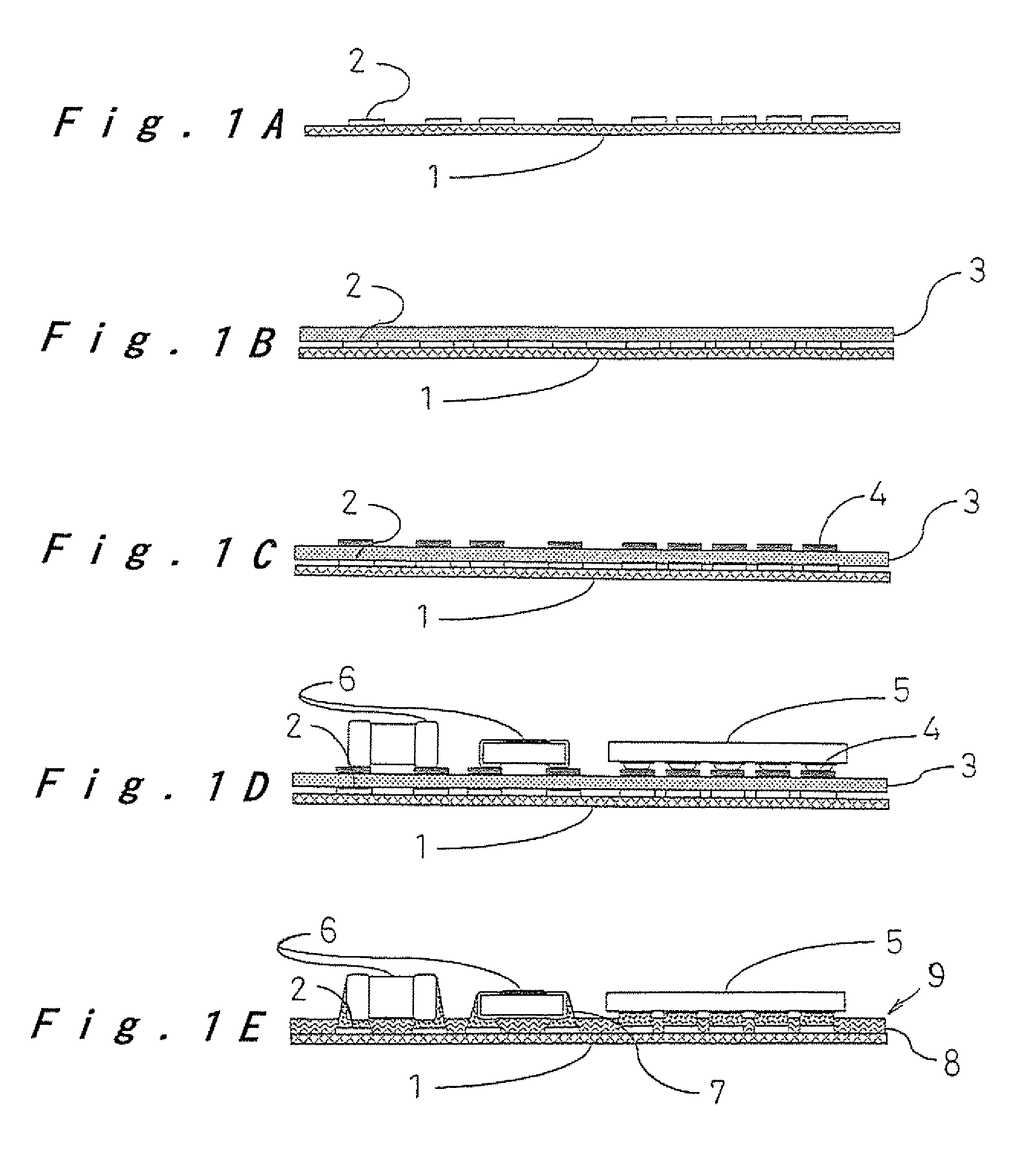
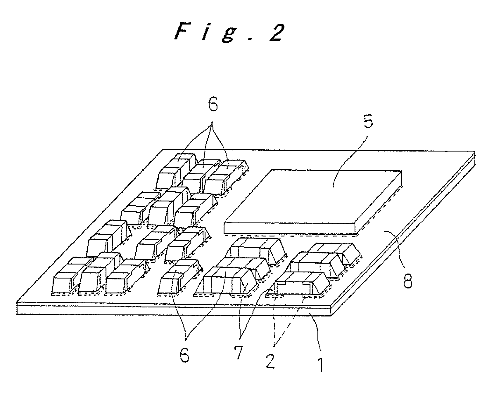
[0061]FIG. 1A to FIG. 1E illustrate process steps of an electronic component mounting method in accordance with a first embodiment of the present invention. This is one embodiment of a component mounting method, in which 1.0×0.5 mm chip components 6 (hereinafter simply referred to as “electronic components 6”) and a WL-CSP (Wafer-Level CSP) 5 with 0.4 mm pitch electrodes (hereinafter simply referred to as “electronic component 5”) are mounted on a circuit substrate 1. Referring to FIG. 1A, the circuit substrate 1 is made of, for example, glass / epoxy resin, and includes gold-plated electrode lands 2 for bonding purposes. A resin sheet 3, which is not hardened vet, is laid on the circuit substrate 1, as shown in FIG. 1B, in a succeeding step. The resin sheet 3 is a 30 μm thick thermosetting resin sheet, which is cut to the same size as the entire circuit substrate 1, and bonded on the circuit substrate 1. The resin sheet 3 may be cut to the size of a region where the electronic compon...

second embodiment

[0068] Next, a second embodiment of the present invention will be described. In the following description of the embodiment, like elements to those of the previous embodiment are given the same reference numerals and will not be described again, and differences only will be described.

[0069] While thermosetting resin was used for the resin sheet 3 in the above-described first embodiment, thermoplastic resin is used in this embodiment for the resin sheet 3. With a thermoplastic resin sheet, the same effect of reinforcing the joints is achieved.

third embodiment

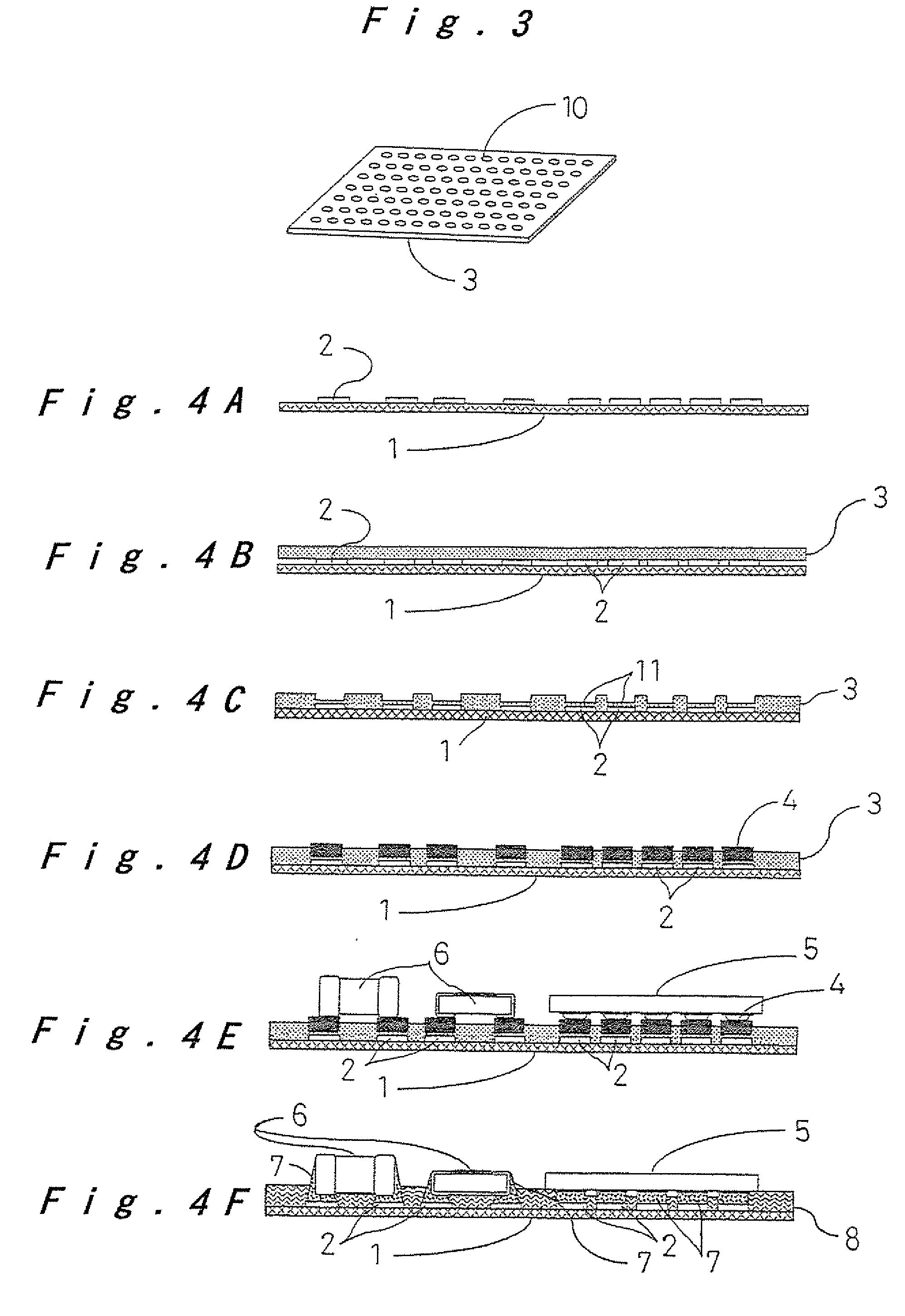
[0070] Next, a third embodiment of the present invention will be described with reference to FIG. 3. In this embodiment, the resin sheet 3 has a matrix of pores 10 with a diameter of, for example, 50 μm arranged at a constant interval of 50 μm. The diameter of the pores 10 may suitably be selected in the range of from several μm which corresponds to the particle size of solder paste 4 to as large as the size of the electrode lands 2.

[0071] In this embodiment, too, with the similar process steps of the first embodiment, the electronic components 5 and 6 are solder-bonded, and the joints are collectively reinforced. As the resin sheet 3 has equally spaced pores 10, it allows molten solder to flow through the pores 10 when the resin sheet 3 is softened in the heating period of about several to 350 seconds during the reflow process. Therefore the electrodes of the electronic components 5 and 6 are readily and reliably bonded to the electrode lands 2 on the circuit substrate 1 even if t...


PUM


Abstract

An electronic component mounting method comprising: supplying an unhardened reinforcing resin on a circuit substrate; supplying a solder paste on bond areas of the circuit substrate on which electrodes of the electronic components are to be bonded; placing the electronic components on the circuit substrate; and heating and then cooling the circuit substrate with the reinforcing resin, the solder paste, and the electronic components carried thereon. The mounting method enables mounting of components with high joint reliability, while incorporating the conventional surface mount process steps. The method may also be applied to the mounting of smaller electronic components with narrower pitch without deteriorating productivity or mounting quality.

Description

TECHNICAL FIELD [0001] The present invention relates to an electronic component mounting method, and more particularly to a method of reinforcing the joints between electronic components and circuit substrate using resin, and to a circuit substrate and a circuit substrate unit on which electronic components have been mounted, which are used in this method. BACKGROUND ART [0002] Surface mount technologies are commonly known as methods of mounting electronic components on a circuit substrate by solder-bonding. The surface mount process usually includes the following steps: [0003] 1. Solder Paste Printing Step [0004] Solder paste, which is the bonding material, is printed on electrode lands of the circuit substrate. [0005] 2. Electronic Component Placing Step [0006] Electronic components are placed such that their electrodes are positioned on the solder paste printed on the electrode lands of the circuit substrate. [0007] 3. Reflow Step [0008] The solder paste is heated and molten so t...

Claims


Application Information

Patent Timeline
Patent Type & Authority Applications(United States)
IPC IPC(8): A47J36/02H05K3/28H05K3/30H05K3/34
CPCH05K3/284H05K3/305H05K3/341H05K3/3436H05K3/3442H05K2203/1105H05K2201/10636H05K2201/10689H05K2201/10977H05K2203/0568H05K3/3484H01L2224/16225H01L2924/19105H05K3/3485Y02P70/50
Inventor MORI, MASATOONISHI, HIROAKIHIRANO, MASATONISHIDA, KAZUTO
Owner PANASONIC CORP
Why Eureka
Try Eureka