Stacked SOI semiconductor devices with back bias mechanism

a semiconductor device and back bias technology, applied in the field of semiconductor devices, can solve the problems of reducing the operating speed of respective transistor elements, reducing the overall lateral dimension, and reducing the packing density of complex semiconductor devices, so as to achieve superior transistor performance, increase the overall packing density, and improve the effect of overall lateral dimension

Active Publication Date: 2019-07-02
GLOBALFOUNDRIES U S INC
View PDF7 Cites 30 Cited by
  • Summary
  • Abstract
  • Description
  • Claims
  • Application Information

AI Technical Summary

Benefits of technology

[0016]Generally, the present disclosure is based on the concept that a stacked SOI architecture may be used, in illustrative embodiments based on a fully depleted transistor configuration, wherein at least two stacked device levels may be implemented, wherein at least the upper SOI device level may have implemented therein a back bias mechanism for providing superior transistor performance. In illustrative embodiments, the back bias mechanism may also be implemented in at least one further SOI device level, thereby contributing to superior transistor performance in at least two stacked SOI device levels and enabling the implementation of well-established planar transistor configurations, while, at the same time, significantly increasing the overall packing density.

Problems solved by technology

Basically, reducing the overall lateral dimensions of transistors and other circuit elements has resulted in an enormous packing density in complex semiconductor devices, wherein several hundred millions of individual transistor elements may be provided in a single semiconductor chip representing a complex central processing unit.
Despite the many advantages associated with the continuous reduction of critical dimensions of semiconductor devices, however, a plurality of side effects accompanying these developments may have to be taken into account so as to not unduly offset the effects obtained by increasing operating speed and packing density.
In other aspects, overall parasitic capacitance in sophisticated transistor elements may contribute to a less than expected performance gain, as, for instance, a non-fully depleted channel region, in combination with the presence of a bulk region, may result in reduced operating speed of respective transistor elements, even if formed on the basis of extremely reduced vertical dimensions of 30 nm and even less.
On the other hand, the implementation of three-dimensional transistor architectures is accompanied by a plurality of sophisticated processes, which may significantly contribute to the overall manufacturing costs.
Although the concept of a fully depleted SOI transistor provides significant performance gain and, thus, allows the configuration of highly complex semiconductor devices, including a large number of transistor elements, it turns out, however, that further reduction of critical dimensions in the area of 30 nm and less may result in significant technical problems that may have to be overcome when striving to further enhance overall packing density of highly complex semiconductor devices.
While, on the other hand, a corresponding increase of packing density on the basis of three-dimensional transistor architectures may be associated with significant technical challenges, as well as with significant manufacturing costs, significant efforts have been made in order to mitigate at least some of the technical problems associated with further device scaling, in particular in planar technologies.
Although the technical approaches disclosed in these prior art documents may aim at enhancing transistor performance based on well-established fully depleted SOI architectures and / or increasing overall packing density, for instance, by contemplating the transfer of semiconductor layers for providing the possibility of forming stacked device configurations, it turns out, however, that these approaches are less than desirable in view of appropriately enhancing packing density while preserving superior transistor controllability, for instance, by using a back bias mechanism.

Method used


Image

  • Stacked SOI semiconductor devices with back bias mechanism
  • Stacked SOI semiconductor devices with back bias mechanism
  • Stacked SOI semiconductor devices with back bias mechanism

Examples


Embodiment Construction

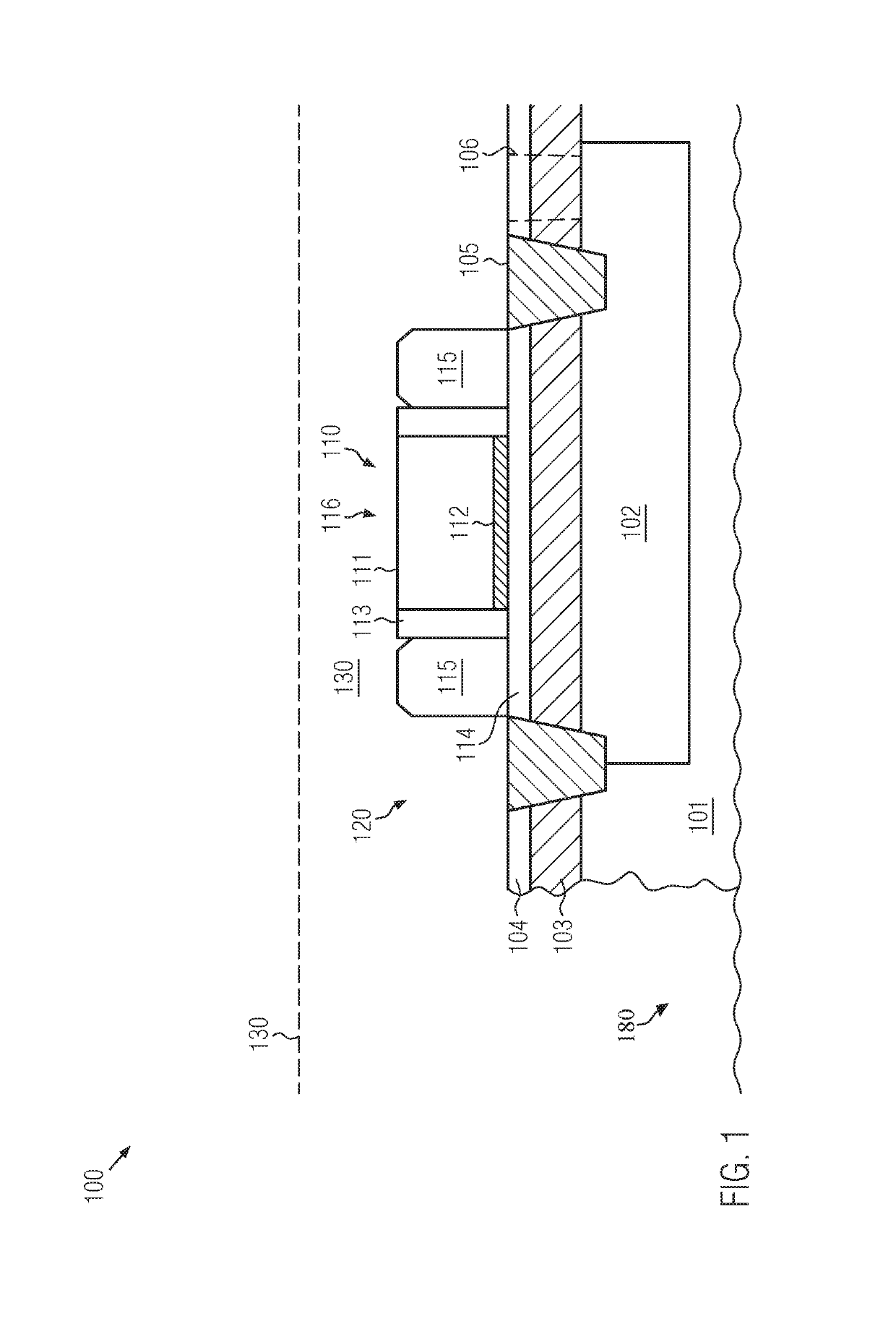
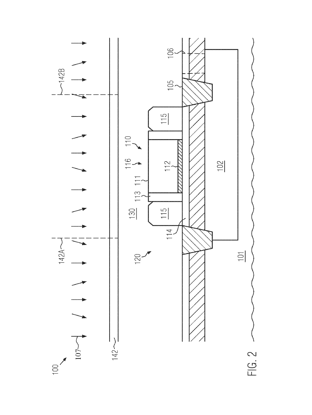
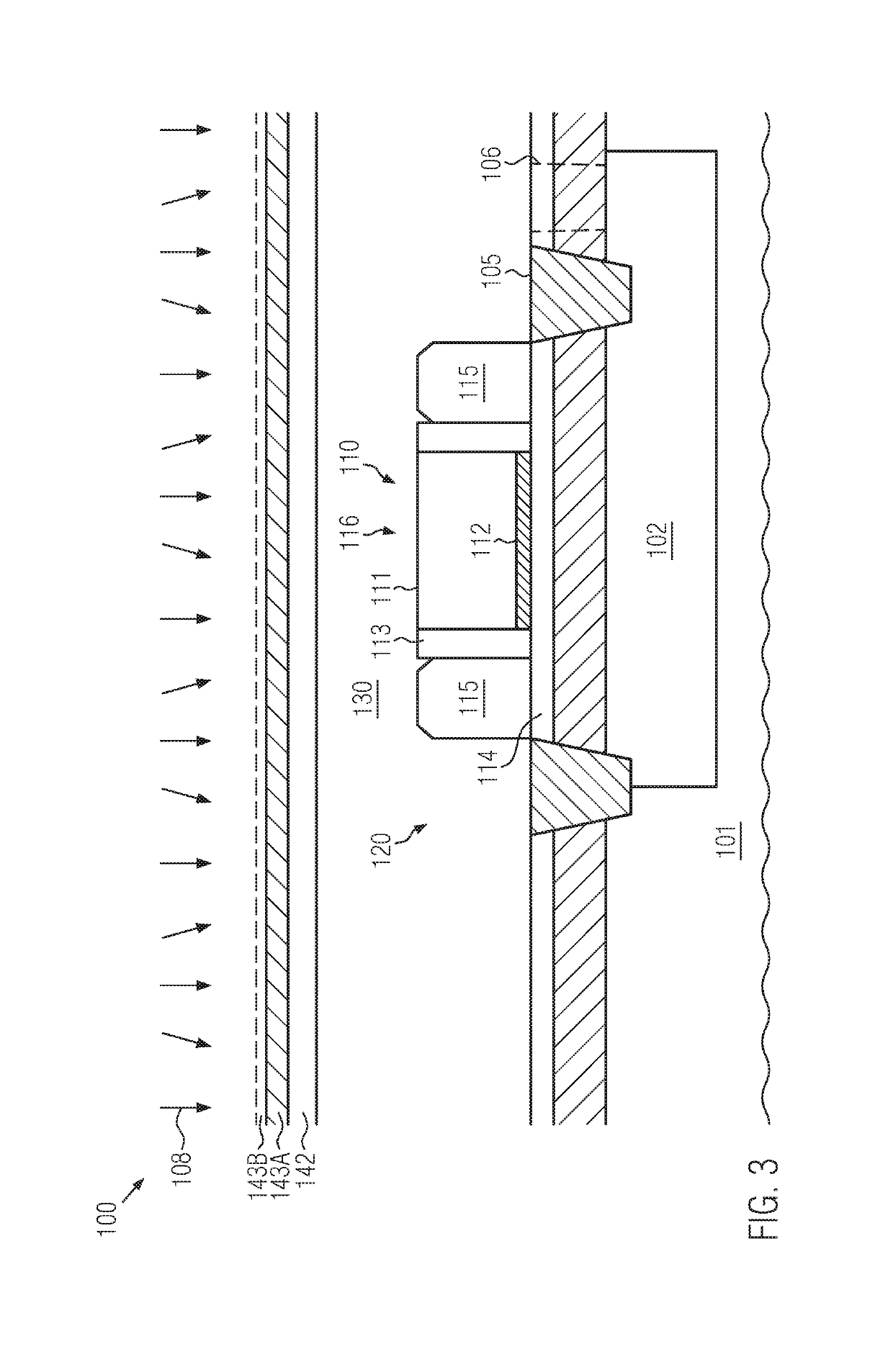
[0030]In the following description, for the purposes of explanation, numerous specific details are set forth in order to provide a thorough understanding of exemplary embodiments. It should be apparent, however, that exemplary embodiments may be practiced without these specific details or with an equivalent arrangement. In other instances, well-known structures and devices are shown in block diagram form in order to avoid unnecessarily obscuring exemplary embodiments. In addition, unless otherwise indicated, all numbers expressing quantities, ratios and numerical properties of ingredients, reaction conditions and so forth used in the specification and claims are to be understood as being modified in all instances by the term “about.”

[0031]Various illustrative embodiments of the invention are described below. In the interest of clarity, not all features of an actual implementation are described in this specification. It will of course be appreciated that in the development of any suc...


PUM


Abstract

A semiconductor device includes at least two stacked SOI levels or configurations, each of which may include transistor elements formed on the basis of a given technology node. At least the uppermost device level may include a back bias mechanism for providing superior controllability of the respective transistor elements. In some illustrative embodiments, at least two of the stacked SOI configurations may have implemented therein a back bias mechanism, wherein an appropriate contact regime is provided so as to connect to the respective conductive regions or layers below the corresponding buried insulating layers for each stacked device level. Consequently, increased lateral packing density may be accomplished on the basis of a given technology node.

Description

BACKGROUND[0001]1. Field of the Disclosure[0002]Generally, the present disclosure relates to the field of semiconductor devices formed on the basis of integration schemes that provide increased overall packing density.[0003]2. Description of the Related Art[0004]Significant progress has been made over the past decades in the field of semiconductor devices by continuously reducing critical dimensions of the individual circuit elements, such as field effect transistors and the like. Basically, reducing the overall lateral dimensions of transistors and other circuit elements has resulted in an enormous packing density in complex semiconductor devices, wherein several hundred millions of individual transistor elements may be provided in a single semiconductor chip representing a complex central processing unit. Implementing reduced lateral dimensions increases the packing density, in particular, in critical device regions, such as static and dynamic RAM (random access memory) regions, w...

Claims


Application Information

Patent Timeline
Patent Type & Authority Patents(United States)
IPC IPC(8): H01L27/01H01L27/12H01L21/84H01L29/06H01L27/06H01L21/822
CPCH01L27/1203H01L21/84H01L29/0649H01L27/0688H01L21/8221H01L21/8234H01L27/088H01L21/823475H01L29/78648H01L29/66628
Inventor PAWLAK, BARTLOMIEJ
Owner GLOBALFOUNDRIES U S INC
Why Eureka
Try Eureka