Compound semiconductor substrate with SiC layer

a technology of compound semiconductor substrate and sic layer, which is applied in the direction of coating, transistor, chemical vapor deposition coating, etc., can solve the problems of warpage of the substrate or cracks the technique of document 1 has a limitation in increasing the thickness of the gan layer,

Active Publication Date: 2019-07-16
AIR WATER INC
View PDF13 Cites 0 Cited by
  • Summary
  • Abstract
  • Description
  • Claims
  • Application Information

AI Technical Summary

Benefits of technology

[0019]According to the present invention, it is possible to provide a compound semiconductor substrate having a desired quality.

Problems solved by technology

On the other hand, the technique of the Document 1 has a limitation in increasing the thickness of the GaN layer, and the withstand voltage has likewise been limited.
This is because when thickening the GaN layer, warpage occurs in the substrate or cracks occur in the GaN layer.
On the other hand, the technique of the Document 2 has a problem that warpage of the substrate tends to occur.
On the other hand, in the technique of the Document 3, there is a problem that warpage of the substrate or crack in the GaN layer easily occurs.

Method used


Image

  • Compound semiconductor substrate with SiC layer
  • Compound semiconductor substrate with SiC layer
  • Compound semiconductor substrate with SiC layer

Examples


first embodiment

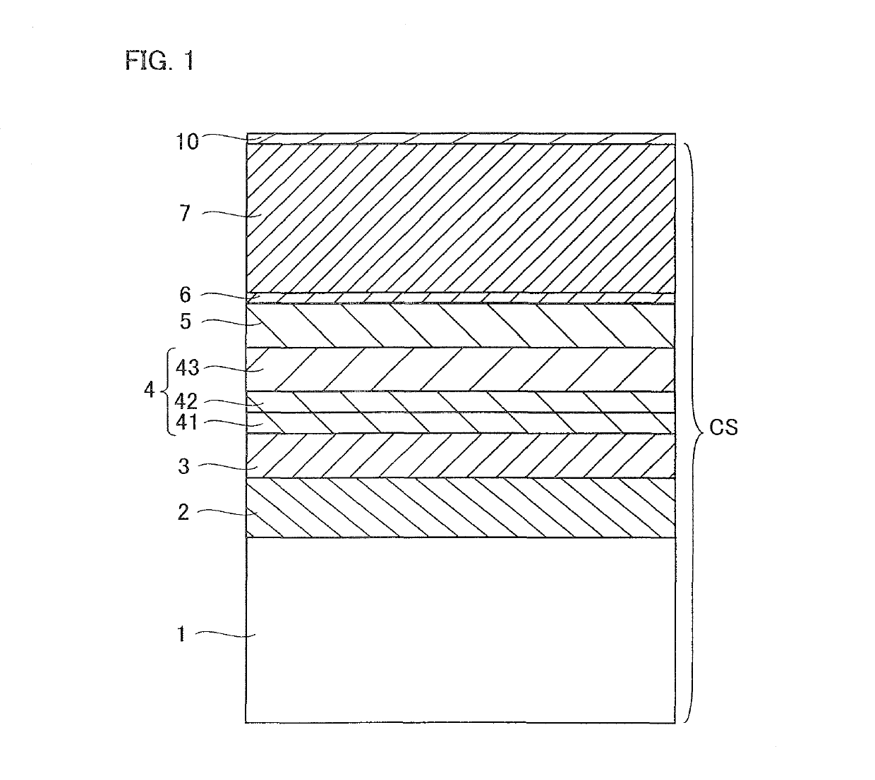
[0025]FIG. 1 is a cross-sectional view showing a configuration of a semiconductor device, according to an embodiment of the present invention.

[0026]Referring to FIG. 1, the semiconductor device in this embodiment includes an HEMT (High Electron Mobility Transistor). The semiconductor device is provided with a compound semiconductor substrate CS and an Al nitride semiconductor layer 10 formed on the compound semiconductor substrate CS.

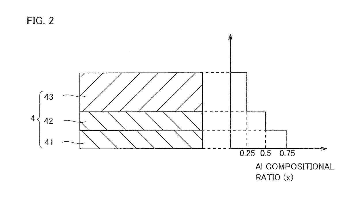
[0027]The compound semiconductor substrate CS is equipped with Si substrate 1, SiC layer 2, AlN buffer layer 3 (an example of an AlN buffer layer), Al nitride semiconductor layer 4 (an example of a nitride semiconductor layer containing Al), GaN layer 5 (an example of a first GaN layer), AlN intermediate layer 6 (an example of a first AlN intermediate layer), and GaN layer 7 (an example of a second GaN layer).

[0028]The Si substrate 1 is made of p+ type Si, for example. The (111) plane is exposed on the surface of Si substrate 1. Note that the Si substra...


PUM

PropertyMeasurementUnit
thicknessaaaaaaaaaa
thicknessaaaaaaaaaa
thicknessaaaaaaaaaa

Abstract

A compound semiconductor substrate having a desired quality is provided.A compound semiconductor substrate has an SiC (silicon carbide) layer, an AlN (aluminum nitride) buffer layer formed on the SiC layer, an Al (aluminum) nitride semiconductor layer formed on the AlN buffer layer, a first GaN (gallium nitride) layer formed on the Al nitride semiconductor layer, a first AlN intermediate layer formed on the first GaN layer in contact with the first GaN layer, and a second GaN layer formed on the first AlN intermediate layer in contact with the first AlN intermediate layer.

Description

TECHNOLOGICAL FIELD[0001]The present invention relates to a compound semiconductor substrate, and more particularly, to a compound semiconductor substrate provided with a SiC (silicon carbide) layer.DESCRIPTION OF THE RELATED ART[0002]GaN (gallium nitride) is known as a wide band gap semiconductor material with a larger band gap and higher insulation breakdown field strength than Si (silicon). Since GaN has higher insulation breakdown resistance than other wide band gap semiconductor materials, it is expected to be applied to next generation low loss power devices.[0003]When an Si substrate is used as a starting substrate (a foundation substrate) of a semiconductor device using GaN, there are a large difference of the lattice constant and a large difference of the coefficient of thermal expansion, between GaN and Si. Due to these differences, phenomena such as warpage occurring on the substrate and cracking in the GaN layer are likely to occur.[0004]As a countermeasure to the warpag...

Claims


Application Information

Patent Timeline
Patent Type & Authority Patents(United States)
IPC IPC(8): H01L31/0328H01L31/0336H01L21/02C23C16/34H01L29/205H01L29/812H01L33/32H01L29/10H01L29/20H01L29/66H01L29/778
CPCH01L21/02447H01L33/32H01L21/0254H01L21/0262H01L21/02381H01L21/02458H01L21/02502H01L29/1029H01L29/2003H01L29/205H01L29/66431H01L29/778H01L29/7787H01L29/812C23C16/34H01L21/02505H01L21/02529H01L2924/10323H01L2924/1033
Inventor NARUKAWA, MITSUHISAFUKAZAWA, AKIRASUZUKI, HIROKIKAWAMURA, KEISUKE
Owner AIR WATER INC
Why Eureka
Try Eureka