Compound semiconductor substrate including electron transition layer and barrier layer

a technology of semiconductor substrate and electron transition layer, applied in the direction of semiconductor devices, basic electric elements, electrical apparatus, etc., can solve the problems of warpage of the substrate, limit to increasing the thickness of the gan layer, limit to withstand voltage as well, etc., and achieve the effect of desired quality

Active Publication Date: 2022-04-26
AIR WATER INC
View PDF18 Cites 0 Cited by
  • Summary
  • Abstract
  • Description
  • Claims
  • Application Information

AI Technical Summary

Benefits of technology

[0021]According to the present invention, a compound semiconductor substrate having desired quality can be provided.

Problems solved by technology

On the other hand, according to the technology of Patent Document 1 etc., there is a limit to increasing the thickness of the GaN layer, and there is a limit to withstand voltage as well.
This is because when a GaN layer is thickened, warpage occurs in substrate and cracks are generated in the GaN layer.

Method used


Image

  • Compound semiconductor substrate including electron transition layer and barrier layer
  • Compound semiconductor substrate including electron transition layer and barrier layer
  • Compound semiconductor substrate including electron transition layer and barrier layer

Examples


first embodiment

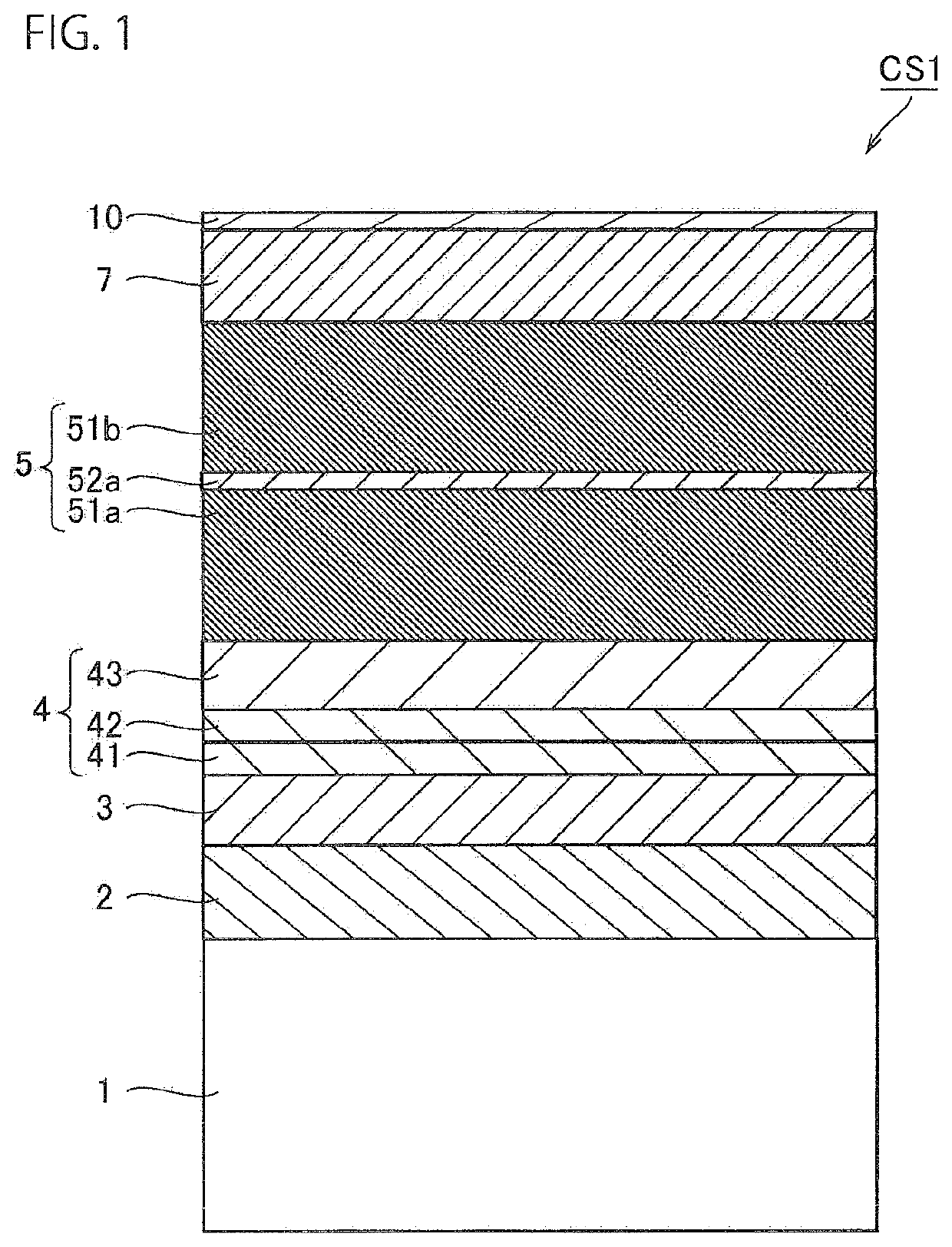
[0031]FIG. 1 is a cross-sectional view showing the configuration of compound semiconductor substrate CS1 in the first embodiment of the present invention.

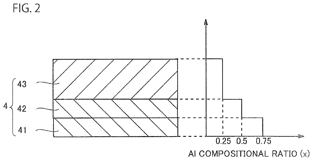
[0032]Referring to FIG. 1, the compound semiconductor substrate CS1 in the present embodiment includes a HEMT (High Electron Mobility Transistor). The compound semiconductor substrate CS1 has Si substrate 1, SiC layer 2, AlN buffer layer 3 (an example of a buffer layer consisting of AlN), Al nitride semiconductor layer 4 (an example of a nitride semiconductor layer including Al), composite layer 5, GaN layer 7 (an example of an electron transition layer), and Al nitride semiconductor layer 10 (an example of a barrier layer).

[0033]Si substrate 1 is made of, for example, p+-type Si. The (111) plane is exposed on the surface of Si substrate 1. Note that Si substrate 1 may have n-type conductivity. Si substrate 1 may be semi-insulating. The (100) plane or the (110) plane may be exposed on the surface of the Si substrate 1. Si substrate...

second embodiment

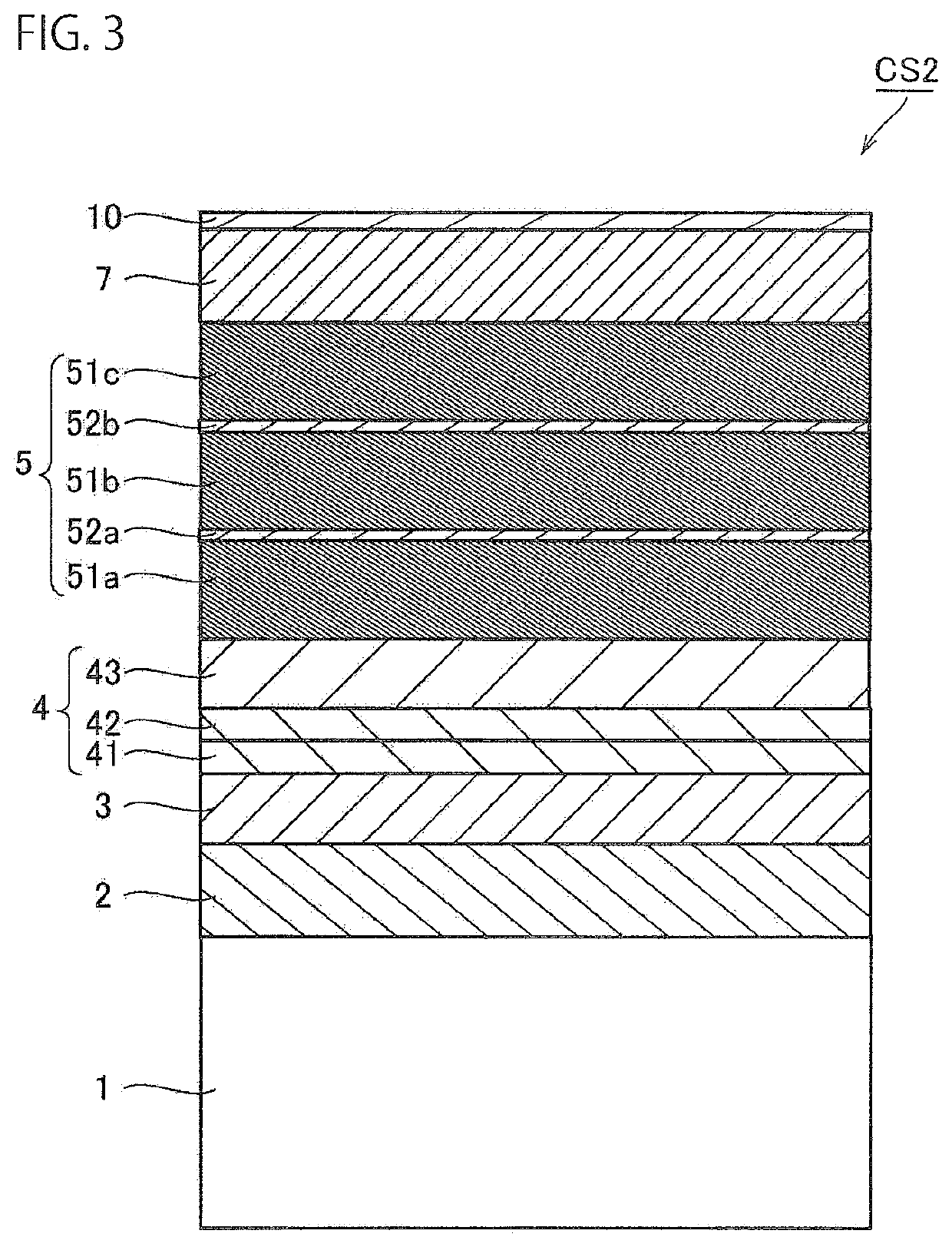
[0059]FIG. 3 is a cross-sectional view showing the configuration of compound semiconductor substrate CS2 in the second embodiment of the present invention.

[0060]Referring to FIG. 3, as compared to the compound semiconductor substrate CS1 in the first embodiment, the compound semiconductor substrate CS2 in the present embodiment is different in the internal configuration of the composite layer 5. Specifically, the composite layer 5 in the present embodiment includes three C—GaN layers 51a, 51b and 51c (an example of a plurality of first layers) as a C—GaN layer, and two AlN layers 52a and 52b (an example of a second layer). The C—GaN layer 51a is the lowest layer among the layers constituting the composite layer 5, and is in contact with the Al nitride semiconductor layer 4. The AlN layer 52a is formed on the C—GaN layer 51a and in contact with the C—GaN layer 51a. The C—GaN layer 51b is formed on the AlN layer 52a and in contact with the AlN layer 52a. The AlN layer 52b is formed on...

example 1

The Invention Example 1

[0079]The inventors of the present invention manufactured compound semiconductor substrate CS1 shown in FIG. 1. The thickness of each of the C—GaN layers 51a and 51b was set to 1450 nanometers, and the thickness of the AlN layer 52a was set to 15 nanometers. The average carbon concentration of each of the C—GaN layers 51a and 51b was set to a value within the range of 1*1019 / cm3 or more and 2*1019 / cm3 or less.


PUM

PropertyMeasurementUnit
thicknessaaaaaaaaaa
thicknessaaaaaaaaaa
thicknessaaaaaaaaaa

Abstract

A compound semiconductor substrate includes a SiC (silicon carbide) layer, a AlN (aluminum nitride) buffer layer formed on the SiC layer, an Al (aluminum) nitride semiconductor layer formed on the AlN buffer layer, a composite layer formed on the Al nitride semiconductor layer, a GaN (gallium nitride) layer as an electron transition layer formed on the composite layer, and an Al nitride semiconductor layer as a barrier layer formed on the GaN layer. The composite layer includes C—GaN layers stacked in a vertical direction, and an AlN layer formed between the C—GaN layers.

Description

TECHNOLOGICAL FIELD[0001]The present invention relates to a compound semiconductor substrate. More particularly, the invention relates to a compound semiconductor substrate with a SiC (silicon carbide) layer.DESCRIPTION OF THE RELATED ART[0002]GaN (gallium nitride) has a larger band gap than Si (silicon). GaN (gallium nitride) is known as a wide band gap semiconductor material, with high isolation breakdown field strength.[0003]As compared to other wide band gap semiconductor materials, GaN has high insulation breakdown resistance. Therefore, GaN is expected to be applied to next-generation low-loss power devices.[0004]When a Si substrate is used as a start substrate (foundation substrate) of a semiconductor device using GaN, a phenomenon in that warpage occurs in the substrate or cracks occur in the GaN layer is likely to occur, due to the large difference in lattice constants and thermal expansion coefficients between GaN and Si.[0005]As a countermeasure to the warpage of the subs...

Claims


Application Information

Patent Timeline
Patent Type & Authority Patents(United States)
IPC IPC(8): H01L29/267H01L21/02H01L29/16H01L29/20H01L29/778
CPCH01L29/267H01L21/0254H01L21/02381H01L21/02447H01L21/02458H01L21/02505H01L21/0262H01L29/1608H01L29/2003H01L29/778H01L29/7786H01L29/207H01L21/02507H01L21/02433H01L29/7783H01L29/812H01L29/66462H01L21/02529H01L2924/05032H01L2924/1033
Inventor NARUKAWA, MITSUHISAOUCHI, SUMITOSUZUKI, HIROKIKAWAMURA, KEISUKE
Owner AIR WATER INC
Why Eureka
Try Eureka