Semiconductor device and method for manufacturing the same

a technology of semiconductor devices and semiconductor substrates, which is applied in the direction of semiconductor devices, semiconductor/solid-state device details, electrical apparatus, etc., can solve the problems of low reliability of connection therewith, low mounting strength on the mounting substrate, and the surface of leads that are not readily wet, so as to improve the reliability of connection with the mounting substrate, and improve the wettability of solder

Active Publication Date: 2019-07-30
ROHM CO LTD
View PDF9 Cites 2 Cited by
  • Summary
  • Abstract
  • Description
  • Claims
  • Application Information

AI Technical Summary

Benefits of technology

[0011]However, with the above-described conventional semiconductor device, whereas the plating layers arranged to improve solder wettability are formed on the lower surfaces of the leads exposed from the sealing resin, plating layers are not formed on the end surfaces of the leads exposed from the sealing resin. The end surfaces of the leads are thus not readily wetted by the cream solder. Therefore with the above-described conventional semiconductor device, there is a problem that mounting strength onto the mounting substrate is low and reliability of connection therewith is low.
[0012]An object of the present invention is to provide a semiconductor device and a method for manufacturing the same by which reliability of connection with a mounting substrate can be improved.
[0013]In order to overcome the previously unrecognized and unsolved challenges described above, a preferred embodiment of the present invention provides a semiconductor device. The semiconductor device includes a semiconductor chip, a plurality of leads, disposed in a periphery of the semiconductor chip, and a sealing resin, sealing the semiconductor chip and the leads such that lower surfaces and outer end surfaces at sides opposite the semiconductor chip of the leads are exposed, and lead plating layers arranged to improve solder wettability are formed on the lower surfaces and the outer end surfaces of the leads.
[0014]With the present arrangement, the lead plating layers arranged to improve solder wettability are formed on the lower surfaces of the leads and the outer end surfaces of the leads and therefore not only the lower surfaces of the leads but the outer end surfaces of the leads are readily wetted by solder. Reliability of connection with a mounting substrate can thereby be improved.
[0023]In the preferred embodiment of the present invention, a die pad, which has an upper surface and a lower surface, with which the semiconductor chip is die bonded to the upper surface, and which is sealed by the sealing resin such that the lower surface is exposed at the lower surface of the sealing resin, and a die pad plating layer, arranged to improve solder wettability and formed on the lower surface of the die pad, are further included.
[0030]By the present manufacturing method, a semiconductor device with which reliability of connection with a mounting substrate can be improved can be manufactured.

Problems solved by technology

However, with the above-described conventional semiconductor device, whereas the plating layers arranged to improve solder wettability are formed on the lower surfaces of the leads exposed from the sealing resin, plating layers are not formed on the end surfaces of the leads exposed from the sealing resin.
The end surfaces of the leads are thus not readily wetted by the cream solder.
Therefore with the above-described conventional semiconductor device, there is a problem that mounting strength onto the mounting substrate is low and reliability of connection therewith is low.

Method used


Image

  • Semiconductor device and method for manufacturing the same
  • Semiconductor device and method for manufacturing the same
  • Semiconductor device and method for manufacturing the same

Examples


Embodiment Construction

[0055]Preferred embodiments of the present invention shall now be described in detail with reference to the attached drawings.

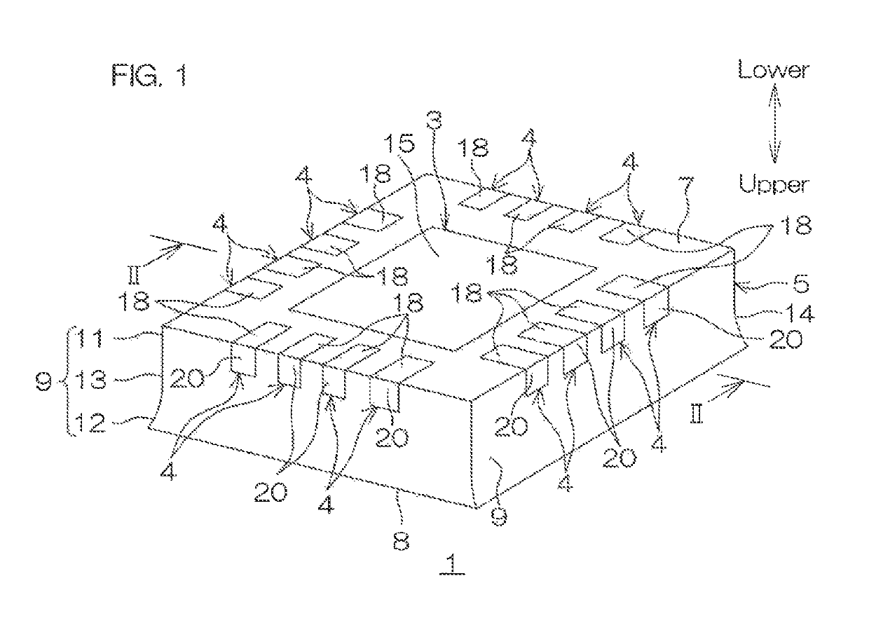
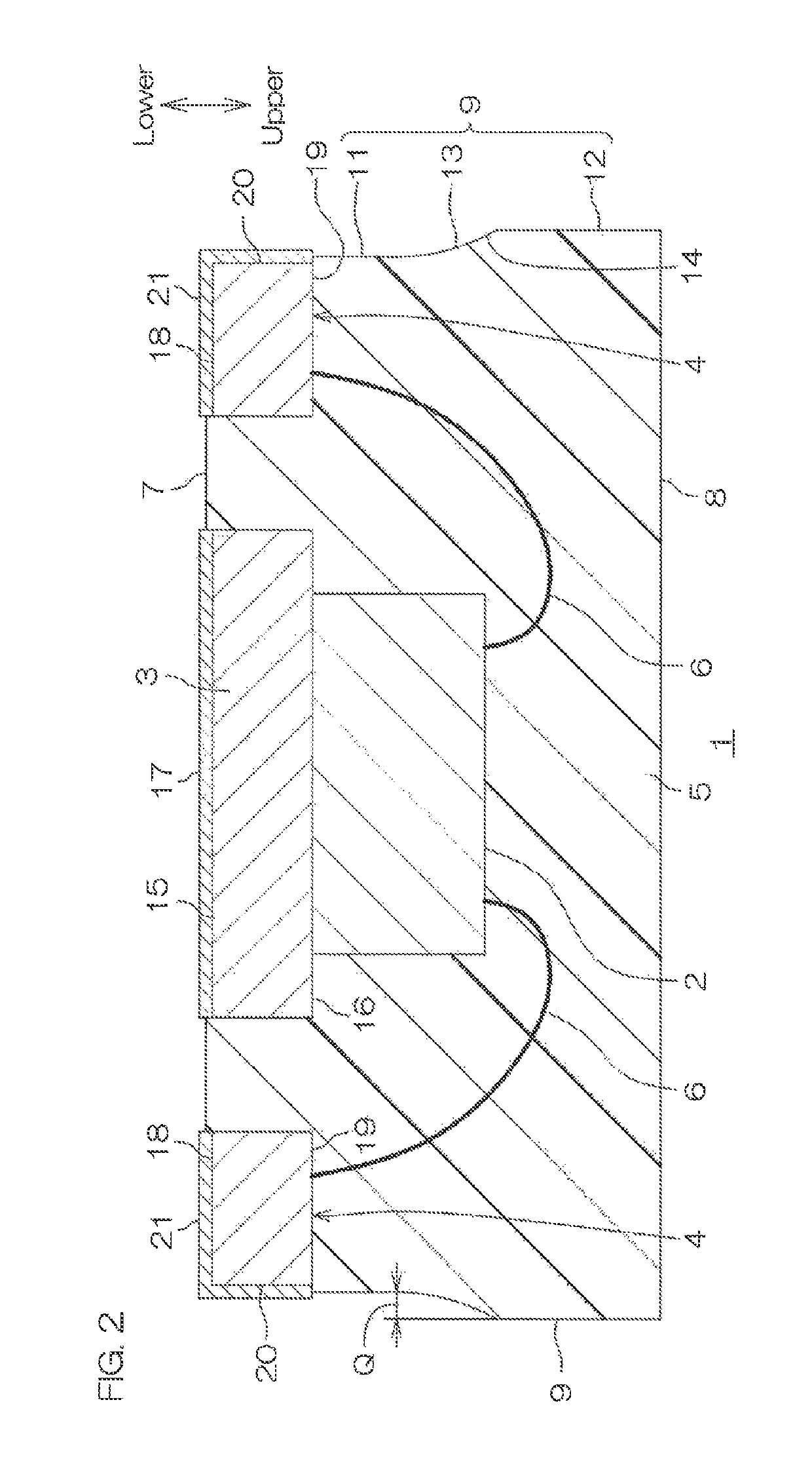
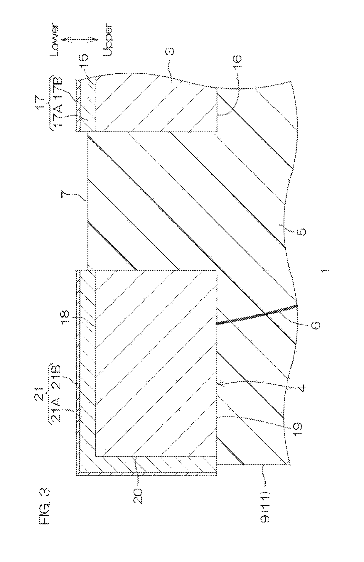
[0056]FIG. 1 is an illustrative perspective view of a semiconductor device according to a first preferred embodiment of the present invention as viewed from obliquely above. Also, FIG. 2 is an illustrative sectional view taken along line II-II in FIG. 1. FIG. 3 is an enlarged view of a portion including a lead at one side and a portion of a die pad of FIG. 2.

[0057]The semiconductor device 1 is a semiconductor device applying a QFN. The semiconductor device 1 includes a semiconductor chip 2, a die pad 3, a plurality of leads 4, and a sealing resin 5. The die pad 3 is arranged to support the semiconductor chip 2. The plurality of leads 4 are electrically connected to the semiconductor chip 2. The sealing resin 5 seals the semiconductor chip 2, the die pad 3, and the plurality of leads 4.

[0058]The semiconductor chip 2 is die bonded onto the die pad 3 in a state ...


PUM


Abstract

A semiconductor device 1 includes a semiconductor chip 2, a plurality of leads 4, disposed in a periphery of the semiconductor chip 2, and a sealing resin 5, sealing the semiconductor chip 2 and the leads 4 such that lower surfaces 18 and outer end surfaces 20 at sides opposite the semiconductor chip 2 of the leads 4 are exposed. Lead plating layers 21 arranged to improve solder wettability are formed on the lower surfaces 18 and the outer end surfaces 20 of the leads 4.

Description

BACKGROUND OF THE INVENTION[0001]1. Field of the Invention[0002]The present invention relates to a semiconductor device and a method for manufacturing the same.[0003]2. Description of the Related Art[0004]With the downsizing of electronic equipment, demand for semiconductor devices applying a QFN (Quad Flat Non-leaded Package) is growing.[0005]A semiconductor device applying a QFN is prepared, for example, by a MAP (molded array packaging) method. With the MAP method, after a plurality of semiconductor chips on a lead frame are sealed in a batch with a sealing resin, cutting apart into individual semiconductor devices, each including a single semiconductor chip, is performed.[0006]The lead frame is constituted, for example, of a metal that contains copper. The lead frame has a lattice-shaped supporting portion. A rectangular die pad and a plurality of leads are formed inside each rectangular region surrounded by the supporting portion. The leads are disposed in a periphery of the di...

Claims


Application Information

Patent Timeline
Patent Type & Authority Patents(United States)
IPC IPC(8): H01L21/48H01L23/498H01L23/495H01L21/56H01L23/31H01L23/00
CPCH01L23/49811H01L21/4842H01L21/4853H01L21/561H01L23/49541H01L23/49582H01L23/49866H01L24/48H01L23/3121H01L2224/48091H01L2924/181H01L23/3107H01L2224/48247H01L2224/97H01L24/45H01L2224/45124H01L2224/45144H01L2224/45147H01L2924/00012H01L2924/00014
Inventor KASUYA, YASUMASA
Owner ROHM CO LTD
Why Eureka
Try Eureka