
Resist underlayer film forming composition containing silicon having ester group

a technology of resisting underlayer film and composition, which is applied in the direction of photomechanical equipment, photosensitive material processing, instruments, etc., can solve the problems of large influence of active ray reflection on a semiconductor substrate, and achieve the effect of satisfying dry etching resistan

Active Publication Date: 2019-08-06
NISSAN CHEM IND LTD
View PDF15 Cites 1 Cited by
  • Summary
  • Abstract
  • Description
  • Claims
  • Application Information

AI Technical Summary

Benefits of technology

[0025]In the present invention, the substrate is coated in such an order that the substrate is coated with the resist underlayer film (containing an inorganic silicon-based compound) formed from the composition of the present invention either with or without an organic underlayer film interposed therebetween, and then the resist underlayer film is coated with a resist film (an organic resist film).
[0026]Then, the resist underlayer film of the present invention functions as a hardmask, and a hydrolyzable group such as an alkoxy group, an acyloxy group, and a halogen group in the structure of a hydrolyzable silane compound of Formula (1) is hydrolyzed or partially hydrolyzed and then, the resultant silanol group is subjected to a condensation reaction to form a polymer having a polysiloxane structure. The polyorganosiloxane structure (intermediate film) is effective as a hardmask for etching an organic underlayer film existing as an underlayer of the intermediate film or for processing (etching) the substrate. That is, the intermediate film has satisfactory dry etching resistance during the substrate processing or against an oxygen-based dry etching gas for etching the organic underlayer film.
[0027]These bonding moieties contained in the polyorganosiloxane structure have a carbon-nitrogen bond or a carbon-oxygen bond, so that the bonding moieties have a dry etching rate by using a halogen-based gas higher than that of a carbon-carbon bond and then, are effective upon transferring a pattern of the upper layer resist to the resist underlayer film.
[0028]Thus, a resist underlayer film formed from the composition of the present invention can enhance the dry etching rate of the resist underlayer film relative to the upper layer resist and possesses dry etching resistance of the resist underlayer film during the substrate processing or the like.
[0029]Accordingly, by using as a hardmask, a polyorganosiloxane produced from a hydrolyzable silane compound of Formula (1) having an ester group (that is, ester bond) or a hydrolyzable silane containing a combination of the hydrolyzable silane compound with a hydrolyzable silane compound of Formula (2) having an amido group (that is, amide bond), a sulfone group (that is, sulfonyl bond), or a phenyl group, where these hydrolyzable silane compounds are contained in the composition of the present invention, when the upper layer resist is exposed to light and is developed with an alkaline developer or an organic solvent, an excellent resist pattern shape can be formed and a rectangular resist pattern can be transferred to an underlayer by dry etching in a subsequent process.MODES FOR CARRYING OUT THE INVENTION
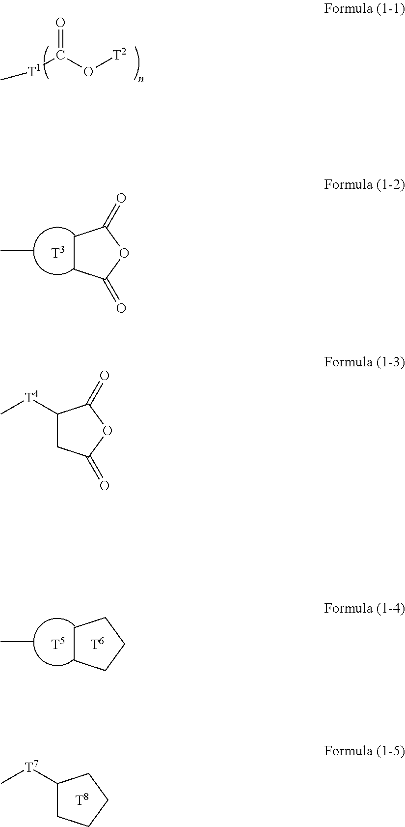
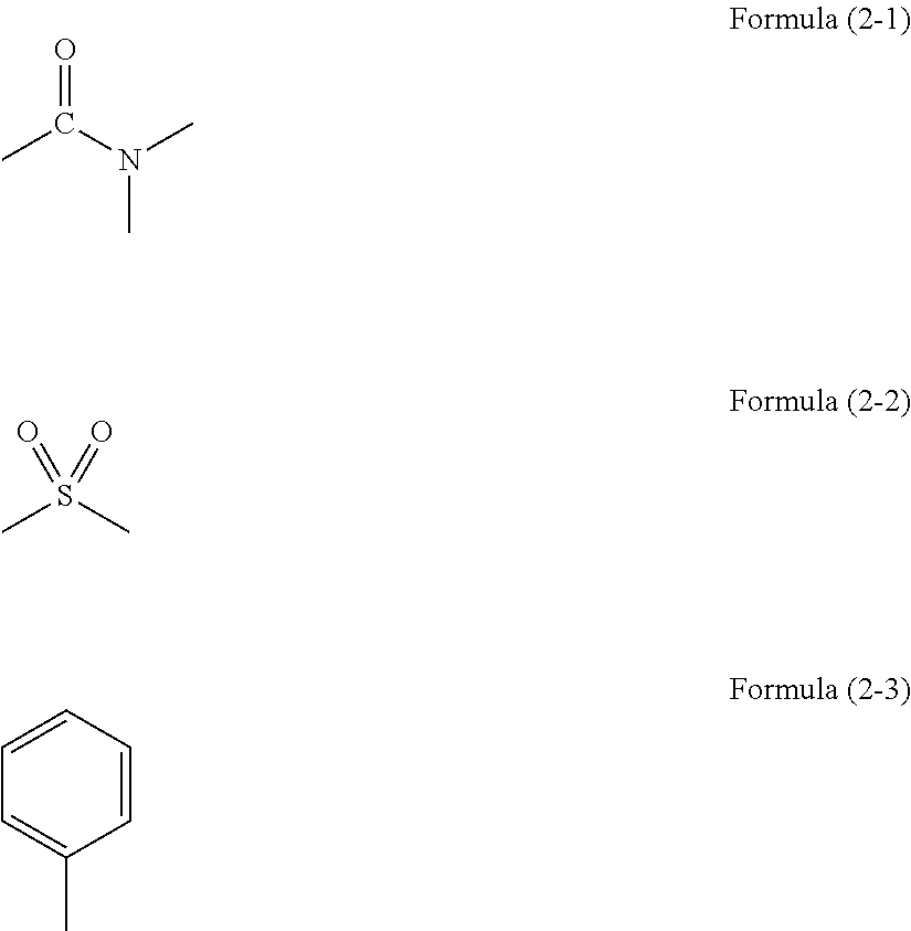
[0030]The present invention provides a resist underlayer film forming composition for lithography characterized by containing as a silane, a hydrolyzable silane, a hydrolysis product thereof, a hydrolysis-condensation product thereof, characterized in that the silane includes a hydrolyzable silane of Formula (1) or a hydrolyzable silane containing a combination of a hydrolyzable silane of Formula (1) with a hydrolyzable silane of Formula (2), and a content of a hydrolyzable silane of Formula (1) or a hydrolyzable silane containing a combination of a hydrolyzable silane of Formula (1) with a hydrolyzable silane of Formula (2) in all silanes is less than 50% by mole.

Problems solved by technology

Following such a tendency, the influence of reflection of active rays on a semiconductor substrate has become a large issue.

Method used


Image

  • Resist underlayer film forming composition containing silicon having ester group
  • Resist underlayer film forming composition containing silicon having ester group
  • Resist underlayer film forming composition containing silicon having ester group

Examples


synthesis example 1

[0203]15.40 g (75 mol % in all silanes) of tetraethoxysilane, 1.23 g (7 mol % in all silanes) of methyltriethoxysilane, 1.37 g (7 mol % in all silanes) of phenyltrimethoxysilane, 1.72 g (6 mol % in all silanes) of methylsulfonyl methylphenyl trimethoxysilane, 1.62 g (5 mol % in all silanes) of (5-(triethoxysilyl)norbornene-2,3-dicarboxylic anhydride, and 32.00 g of acetone were charged into a 100 mL flask. While the resultant mixture solution was stirred with a magnetic stirrer, 6.66 g of a 0.01 mol / L hydrochloric acid was added dropwise into the mixture solution. After the completion of the addition, the flask was transferred into an oil bath adjusted to 85° C., and under warming-reflux, the reaction was effected for 240 minutes. Then, the reaction solution was cooled down to room temperature and to the reaction solution, 21 g of propylene glycol monomethyl ether acetate was added. From the resultant reaction solution, ethanol as a reaction by-product, water, and hydrochloric acid ...

synthesis example 2

[0204]15.48 g (75 mol % in all silanes) of tetraethoxysilane, 1.24 g (7 mol % in all silanes) of methyltriethoxysilane, 1.37 g (7 mol % in all silanes) of phenyltrimethoxysilane, 1.73 g (6 mol % in all silanes) of methylsulfonyl methylphenyl trimethoxysilane, 1.51 g (5 mol % in all silanes) of 3-(triethoxysilyl)propylsuccinic anhydride, and 31.98 g of acetone were charged into a 100 mL flask. While the resultant mixture solution was stirred with a magnetic stirrer, 6.69 g of a 0.01 mol / L hydrochloric acid was added dropwise into the mixture solution. After the completion of the addition, the flask was transferred into an oil bath adjusted to 85° C., and under warming-reflux, the reaction was effected for 240 minutes. Then, the reaction solution was cooled down to room temperature and to the reaction solution, 21 g of propylene glycol monomethyl ether acetate was added. From the resultant reaction solution, ethanol as a reaction by-product, water, and hydrochloric acid were distilled...

synthesis example 3

[0205]15.44 g (75 mol % in all silanes) of tetraethoxysilane, 1.23 g (7 mol % in all silanes) of methyltriethoxysilane, 1.37 g (7 mol % in all silanes) of phenyltrimethoxysilane, 1.72 g (6 mol % in all silanes) of methylsulfonyl methylphenyl trimethoxysilane, 1.56 g (5 mol % in all silanes) of the compound 1, and 31.99 g of acetone were charged into a 100 mL flask. While the resultant mixture solution was stirred with a magnetic stirrer, 6.68 g of a 0.01 mol / L hydrochloric acid was added dropwise into the mixture solution. After the completion of the addition, the flask was transferred into an oil bath adjusted to 85° C., and under warming-reflux, the reaction was effected for 240 minutes.

[0206]Then, the reaction solution was cooled down to room temperature and to the reaction solution, 21 g of propylene glycol monomethyl ether acetate was added. From the resultant reaction solution, ethanol as a reaction by-product, water, and hydrochloric acid were distilled off under reduced pres...


PUM

PropertyMeasurementUnit
molar ratioaaaaaaaaaa

Abstract

A resist underlayer film forming composition for lithography for a resist underlayer film usable as a hardmask. A resist underlayer film forming composition for lithography, including: as a silane, a hydrolyzable silane, a hydrolysis product thereof, or a hydrolysis-condensation product thereof, wherein the hydrolyzable silane includes a hydrolyzable silane of Formula (1) or a hydrolyzable silane containing a combination of a hydrolyzable silane of Formula (1) with a hydrolyzable silane of Formula (2), and a content of the hydrolyzable silane of Formula (1) or the hydrolyzable silane containing a combination of a hydrolyzable silane of Formula (1) with a hydrolyzable silane of Formula (2) in all silanes is less than 50% by mole,R1aR2bSi(R3)4−(a+b)  Formula (1)R4a1R5b1Si(R6)4−(a1+b1)  Formula (2).

Description

TECHNICAL FIELD[0001]The present invention relates to a composition for forming an underlayer film between a substrate and a resist (for example, a photoresist and an EUV resist) that are used in the production of semiconductor devices. More in detail, the present invention relates to a resist underlayer film forming composition for lithography for forming an underlayer film used for an underlayer of a photoresist in a lithography process of the production of semiconductor devices. In addition, the present invention relates to a forming method of a resist pattern using the underlayer film forming composition.BACKGROUND ART[0002]Conventionally, in the production of semiconductor devices, fine processing by lithography using a photoresist has been performed. The fine processing is a processing method for forming fine convexo-concave shapes corresponding to the following pattern on the surface of a substrate by: forming a thin film of a photoresist on a semiconductor substrate such as ...

Claims


Application Information

Patent Timeline
Patent Type & Authority Patents(United States)
IPC IPC(8): G03F7/075G03F7/36G03F7/30G03F7/32C08G77/26C08G77/00C08G77/14H01L21/033C08G77/28C09D183/08C09D183/06G03F7/09H01L21/02G03F7/40
CPCG03F7/0757H01L21/0332C08G77/26C08G77/28C08G77/80C09D183/06C09D183/08G03F7/0752G03F7/091G03F7/094G03F7/30G03F7/322G03F7/325G03F7/36G03F7/40H01L21/02126H01L21/02282C08G77/14
Inventor KANNO, YUTANAKAJIMA, MAKOTOTAKEDA, SATOSHIWAKAYAMA, HIROYUKI
Owner NISSAN CHEM IND LTD
Learn More