Resistive memory device having a retention layer

Active Publication Date: 2019-08-13
4D S
View PDF17 Cites 4 Cited by
  • Summary
  • Abstract
  • Description
  • Claims
  • Application Information

AI Technical Summary

Benefits of technology

[0022]Implementations may include one or more of the following features. The method where the memory device further includes a template layer between the bottom electrode and the memory layer, where the crystalline structure of the memory layer matches the crystalline structure of the template layer, and where the first current is additionally conducted through the template layer. The method where the conductivity of the template layer is greater than 10×106 s m-1. The method where the memory device further includes: a first barrier layer, configured to substantially prevent the conduction of ions or vacancies therethrough, where the top electrode is between the first barrier layer and the retention layer; and a second barrier layer, configured to substantially prevent the

Problems solved by technology

DRAM, however, is expensive and volatile (for example, the data may need to be refreshed every 60 milliseconds) and sacrifices retention to maximize speed and endurance.
NAND Flash, however, sacrifices both speed and endurance to maximize retention.
Being limited to two dimensions (2D), DRAM will likely remain expensive since silicon area largely defines cost per gigabyte.
In contrast, the cost of NAND Flash is expected to decline over time because of three dimensional (3D) stacking.
The cost gap between DRAM and NAND Flash will likely increase over time.
It is equally unlikely that any emerging memory technology will replace DRAM because its speed and endurance combination is exceptionally hard to beat.
Furthermore, there i

Method used


Image

  • Resistive memory device having a retention layer
  • Resistive memory device having a retention layer
  • Resistive memory device having a retention layer

Examples


Example

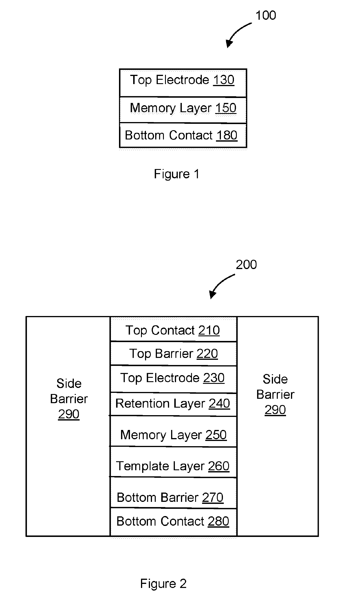
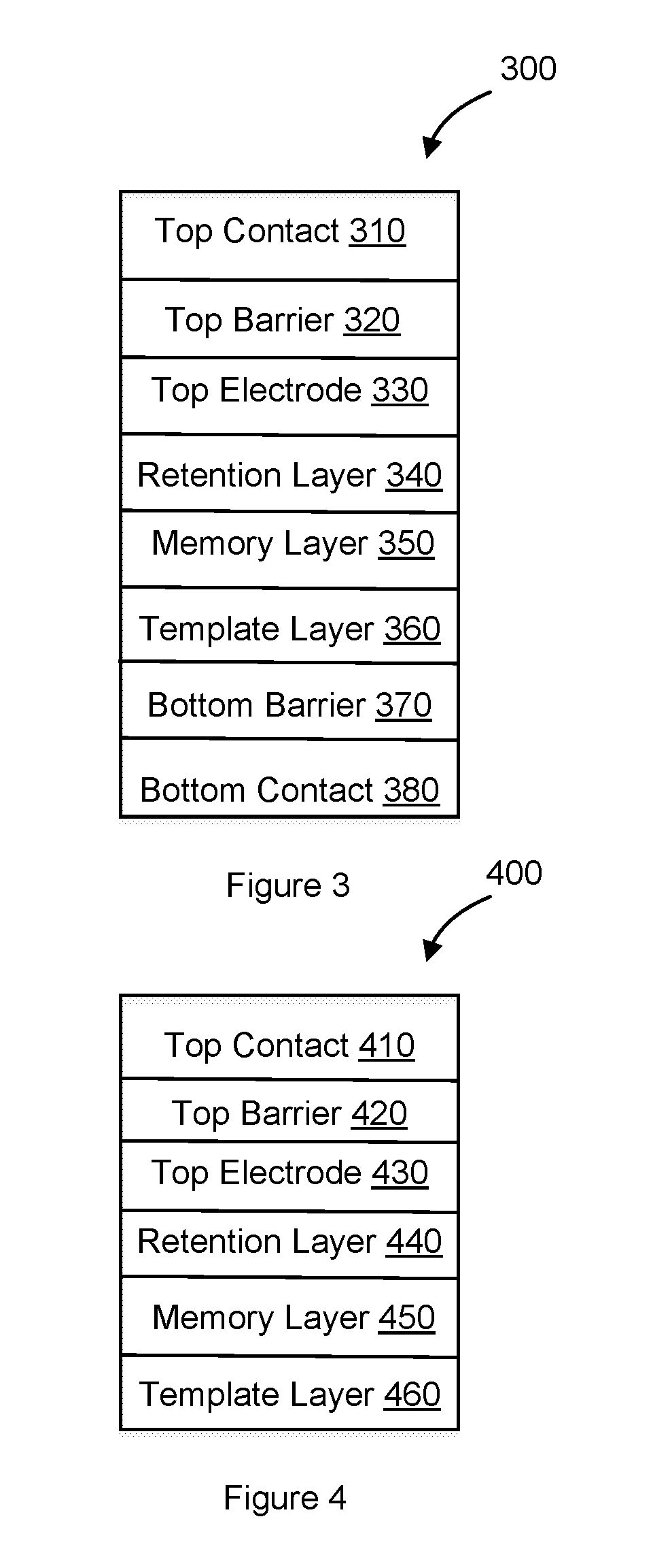
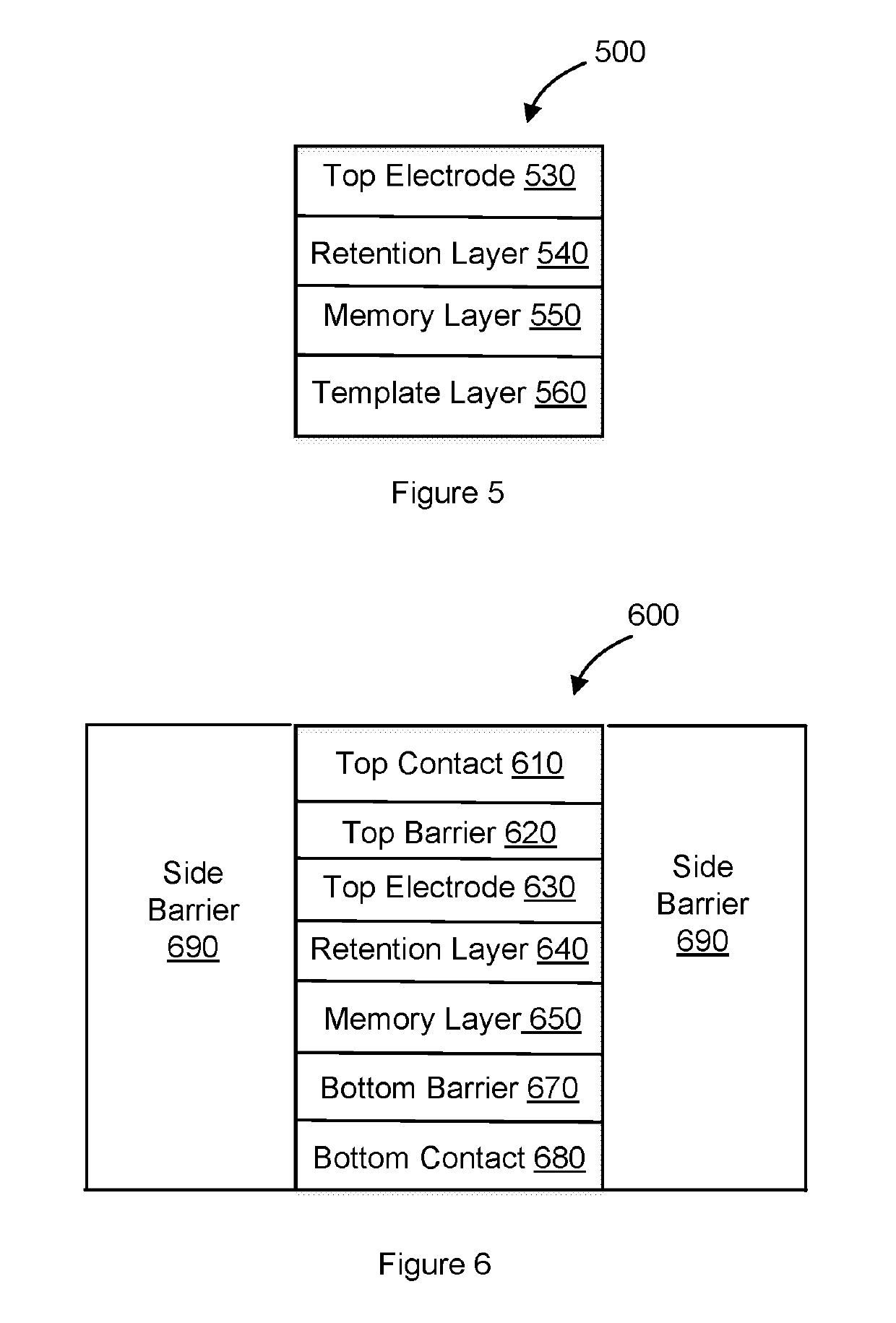
[0031]Particular embodiments of the invention are illustrated herein in conjunction with the drawings.

[0032]Various details are set forth herein as they relate to certain embodiments. However, the invention can also be implemented in ways which are different from those described herein. Modifications can be made to the discussed embodiments by those skilled in the art without departing from the invention. Therefore, the invention is not limited to particular embodiments disclosed herein.

[0033]The present invention is related to a nonvolatile memory device. The memory device can be utilized in a variety of applications from a free standing nonvolatile memory to an embedded device in a variety of applications. These applications include but are not limited to embedded memory used in a wide range of SOC (system on chip), switches in programmable or configurable ASIC, solid state drive used in computers and servers, memory sticks used in mobile electronics like camera, cell phone, iPod®...


PUM


Abstract

A memory device is disclosed. The memory device includes a bottom electrode. The memory device also includes a memory layer connected to the bottom electrode, where the memory layer has a variable resistance. The memory device also includes a conductive top electrode on the memory layer, where the top electrode and the memory layer cooperatively form a heterojunction memory structure. The memory device also includes a retention layer between the memory layer and the top electrode, where the retention layer has a variable ionic conductivity, where the retention layer is configured to selectively resist ionic conduction, and where the resistivity of the retention layer is less than 1×10⁻⁴ ohm-m.

Description

FIELD OF THE INVENTION[0001]The present invention relates generally to nonvolatile memory devices, and more particularly to memory devices having effective speed comparable to DRAM, which do not require speed-crippling error correction and include hetero junctions of oxide materials.BACKGROUND OF THE INVENTION[0002]In general, memory devices or systems can be segmented in 3 distinct categories: internet-of-things (IoT) memories, embedded memories, and high-density high-volume memories. The memory requirements (cost, density, speed, endurance, retention, power consumption) are quite different for each of these 3 categories.[0003]IoT memories tend to be inexpensive, power-efficient, and low-density. Memories embedded in complex system chips tend to be fast, area-efficient, and medium-density. High-density high-volume memories must be scalable to small geometries to be cost effective.[0004]The high-density high-volume memory category is currently dominated by DRAM (which is volatile) a...

Claims


Application Information

Patent Timeline
IPC IPC(8): H01L29/267H01L45/00G11C13/00
CPCH01L45/1233G11C13/004G11C13/0007G11C13/0069H01L45/08H01L45/1246H01L45/1266H01L45/147H01L45/1608G11C2013/009G11C2013/0045G11C2213/13G11C2213/31G11C2213/51G11C2213/52G11C2213/55H10N70/801H10N70/24H10N70/8836H10N70/021H10N70/826H10N70/828H10N70/8416
Inventor DESU, SESHUBABUVAN BUSKIRK, MICHAEL
Owner 4D S
Why Eureka
Try Eureka