Optical module

a technology of optical modules and optical coupling, applied in the field of optical modules, can solve the problems of poor optical coupling characteristics, affecting the manufacturing yield, and disadvantageous rising costs, and achieve the effect of convenient optical axis adjustmen

Active Publication Date: 2019-08-13
LUMENTUM JAPAN INC
View PDF11 Cites 2 Cited by
  • Summary
  • Abstract
  • Description
  • Claims
  • Application Information

AI Technical Summary

Benefits of technology

[0007]This aims to provide optical modules assembled from fewer components and easier for optical axis adjustment.
[0009]With the reflector monolithically integrated in the semiconductor laser, only fewer components may be necessary. With the lens and the semiconductor laser independently separated, the optical axis adjustment may be easier in such a way as positioning during actual light transmission and reception.

Problems solved by technology

The semiconductor laser, when manufactured with the reflector and the lens positioned in an undesired position relationship, has poor optical coupling characteristics, due to an undesired emitting angle of the emitting light from the semiconductor laser.
Besides, due to unchangeability of positions of the reflector and the lens after the manufacture, the semiconductor lasers for the worse may be unavailable for use, possibly affecting their manufacturing yield.
Besides, an increased number of components and manufacturing processes are necessary, leading to disadvantageous rising costs.

Method used


Image

  • Optical module
  • Optical module
  • Optical module

Examples


Embodiment Construction

[0021]Hereinafter, embodiments will be described specifically and in detail with reference to drawings. In all the drawings for describing the embodiments, the same reference numerals are assigned to members having the same function and repetitive description thereof will be omitted. The following drawings merely illustrate examples of the embodiments, and sizes of the drawings and scales described in the examples do not necessarily coincide with each other.

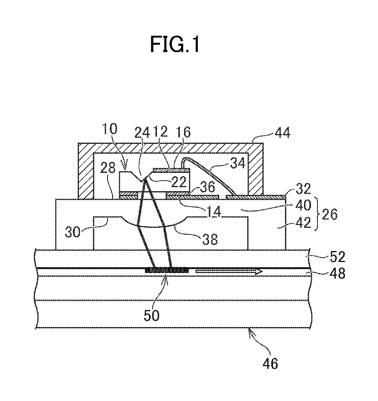
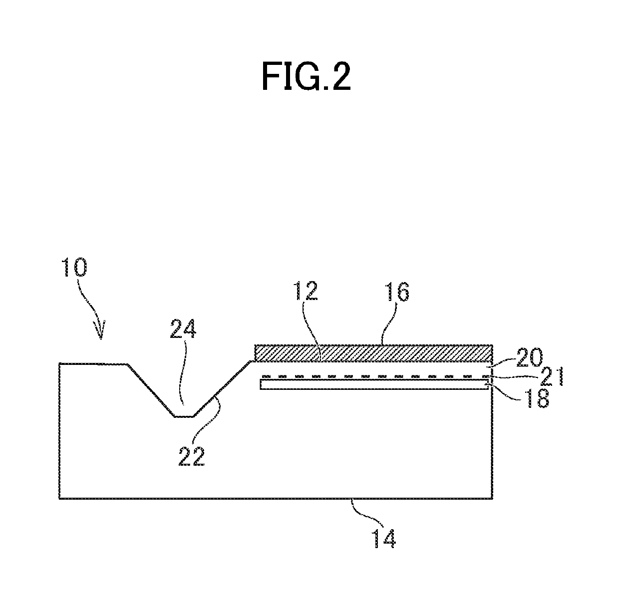
[0022]FIG. 1 is a longitudinal sectional view of an optical module in accordance with an embodiment. The optical module includes a semiconductor laser 10. The semiconductor laser 10 is a distributed feedback (DFB) laser and is capable of emitting light of a single wavelength (e.g. 1.3 μm). The DFB laser is suited to a signal source for long-distance large-capacity optical communication because of its single mode oscillation. The semiconductor laser 10 may be not only the DFB laser but also a distributed Bragg reflector (DBR) lase...


PUM


Abstract

An optical module includes a semiconductor laser with an active layer disproportionately positioned closer to the first surface. The semiconductor laser includes a reflector for reflecting the light outgoing from the active layer in a direction along the first surface toward another direction. The active layer and the reflector are monolithically integrated in the semiconductor laser. The optical module includes a carrier formed from a light transmissive material and having a third surface and a fourth surface opposite to each other. The semiconductor laser is mounted on the carrier so as for the light to enter the third surface. The carrier has a lens integrally on the fourth surface. The optical module includes a substrate having an optical waveguide and an optical coupler for guiding the light to the optical waveguide. The optical waveguide and the optical coupler are integrated in the substrate.

Description

CROSS-REFERENCE TO RELATED APPLICATION[0001]The present application claims priority from Japanese application JP2017-075093 filed on Apr. 5, 2017, the content of which is hereby incorporated by reference into this application.BACKGROUND OF THE INVENTION1. Field of the Invention[0002]This relates to optical modules.2. Description of the Related Art[0003]To transmit oscillation light generated from a semiconductor laser, techniques by means of a silicon waveguide with a grating coupler have begun to be used, instead of direct optical coupling to an optical fiber. JP2014-110257A discloses a semiconductor laser including a reflector for diverting horizontally-oscillated light toward a back side and a lens for focusing the reflection light, both integrally built in a semiconductor substrate. The semiconductor laser is mounted on a surface of a submount on an opposite side to the lens.[0004]To obtain good optical coupling characteristics, the light focused by the lens should have a beam w...

Claims


Application Information

Patent Timeline
Patent Type & Authority Patents(United States)
IPC IPC(8): H01S5/026G02B6/42H01S5/022H01S5/062H01S5/10H01S5/18H01S5/12
CPCH01S5/0267G02B6/4206G02B6/4214H01S5/0228H01S5/0261H01S5/0623H01S5/18H01S5/02216H01S5/02276H01S5/02288H01S5/1085H01S5/12G02B2006/12107G02B2006/12147H01S5/0225H01S5/02253H01S5/02345
Inventor SUZUKI, TAKANORITANAKA, SHIGEHISA
Owner LUMENTUM JAPAN INC
Why Eureka
Try Eureka