

Nonvolatile protein memory system with optical write/erase and electrical readout capability
a protein memory and optical write/erase technology, applied in the field can solve the problems of limited bottom-up process by self-assembly, difficult interfacing with an external device, and inconvenient fabrication of nonvolatile protein memory systems, so as to reduce the power of the system and facilitate the fabrication of the nonvolatile protein memory system
- Summary
- Abstract
- Description
- Claims
- Application Information
AI Technical Summary
Benefits of technology
Problems solved by technology
Method used
Image

Examples
Embodiment Construction
[0027]Hereinafter, the present invention will be described more fully with reference to the accompanying drawings, in which example embodiments of the invention are shown.
[0028]As those skilled in the art would realize, the described embodiments may be modified in various different ways, all without departing from the spirit or scope of the present invention. Parts that are irrelevant to the description will be omitted to clearly describe the present invention, and the same or similar constituent elements will be designated by the same reference numerals throughout the specification. In addition, detailed description of widely known technologies will be omitted.
[0029]In addition, unless explicitly described to the contrary, the word “comprise” and variations such as “comprises” or “comprising” will be understood to imply the inclusion of stated elements but not the exclusion of any other elements.
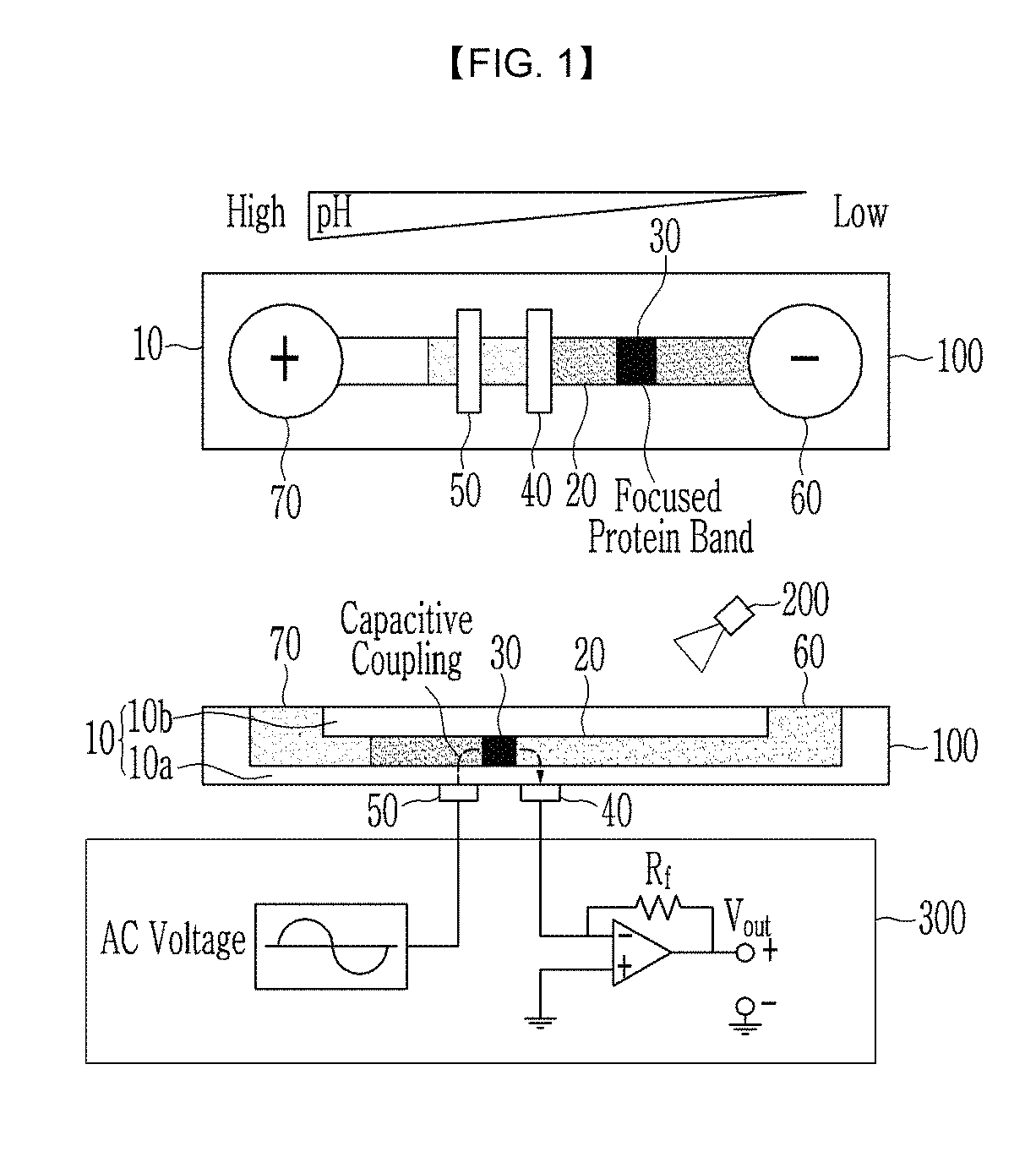
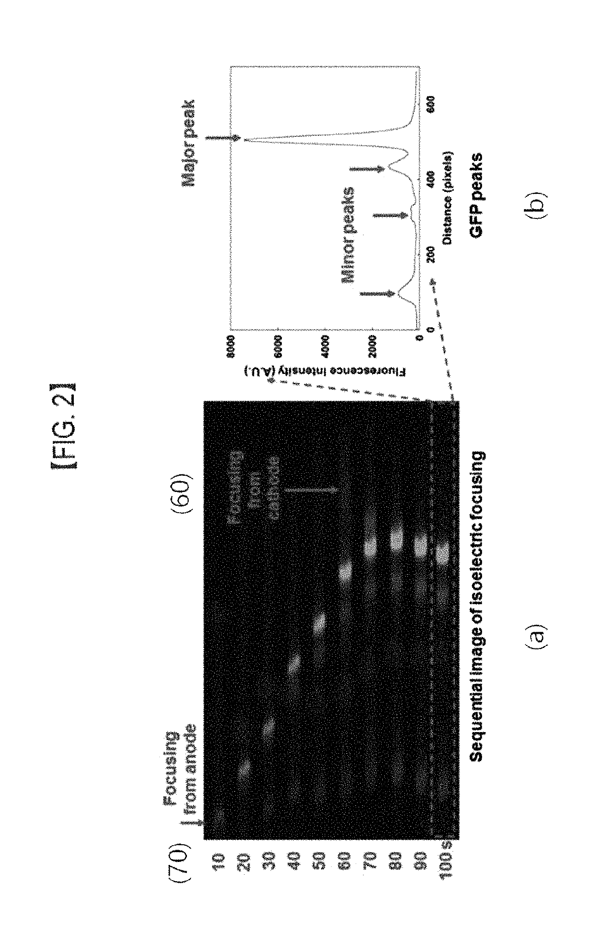
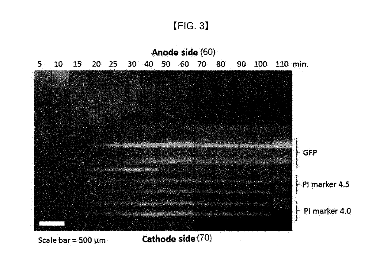
[0030]FIG. 1 shows a schematic plane view and a schematic cross-sectional view of a non...
PUM
| Property | Measurement | Unit |
|---|---|---|
| thickness | aaaaa | aaaaa |
| thickness | aaaaa | aaaaa |
| voltage | aaaaa | aaaaa |
Abstract
Description
Claims
Application Information