Method and apparatus of processing wafers with compressive or tensile stress at elevated temperatures in a plasma enhanced chemical vapor deposition system
What is AI technical title?
AI technical title is built by Patsnap AI team. It summarizes the technical point description of the patent document.
a chemical vapor deposition and elevated temperature technology, applied in the direction of electrostatic holding devices, electric apparatus, basic electric elements, etc., can solve the problems of substrate deformation, contamination and other troubles of subsequent process steps, non-uniformity of process surface, etc., and achieve the effect of sufficient attenuation
Active Publication Date: 2019-09-03
APPLIED MATERIALS INC
View PDF60 Cites 5 Cited by
Summary
Abstract
Description
Claims
Application Information
AI Technical Summary
This helps you quickly interpret patents by identifying the three key elements:
Problems solved by technology
Method used
Benefits of technology
Benefits of technology
The patent text describes a device called the ESC (Electrostatic Chuck) that is used to hold semiconductor devices in place during processing. The ESC is made of a special material that has good insulation properties and is able to hold a static charge. The device also has protective circuitry to prevent harmful electricity from damaging the device. The technical effect of the patent is to provide a better and more reliable method for holding semiconductor devices during processing.
Problems solved by technology
One problem that occurs during plasma processing is deformation of a substrate being processed, especially for a device substrate, i.e. a patterned substrate at high temperatures.
Bowing of the substrate may lead to non-uniformity of the process surface.
Sides and back of a bowed substrate may be processed which not only wastes processing material, as precursors for plasma processing are usually very expensive, but also causes contaminations and other troubles for subsequent process steps.
In such a case, a chucked substrate may still become deformed during a plasma process due to high operating temperature.
Method used
Image
Click on the blue label to locate the original text in one second.
Reading with bidirectional positioning of images and text.
Examples
Embodiment Construction
Exemplary Chamber Hardware
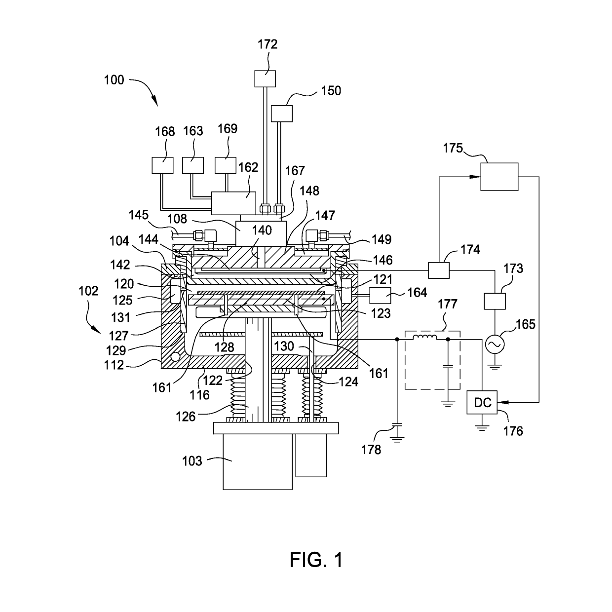
[0026]FIG. 1 illustrates a cross sectional view of a PECVD system 100 in accordance with the present disclosure. It should be noted that although a PECVD system is described in this application, apparatus and method of the present disclosure may apply to any suitable plasma process using an electrostatic chuck. The PECVD system 100 generally comprises a chamber body 102 supporting a chamber lid 104 which may be attached to the chamber body 102 by a hinge. The chamber body 102 comprises sidewalls 112 and a bottom wall 116 defining a processing region 120. The chamber lid 104 may comprise one or more gas distribution systems 108 disposed therethrough for delivering reactant and cleaning gases into the processing region 120. A circumferential pumping channel 125 formed in the sidewalls 112 and coupled to a pumping system 164 is configured for exhausting gases from the processing region 120 and controlling the pressure within the processing region 120. Two pass...
PUM
Abstract
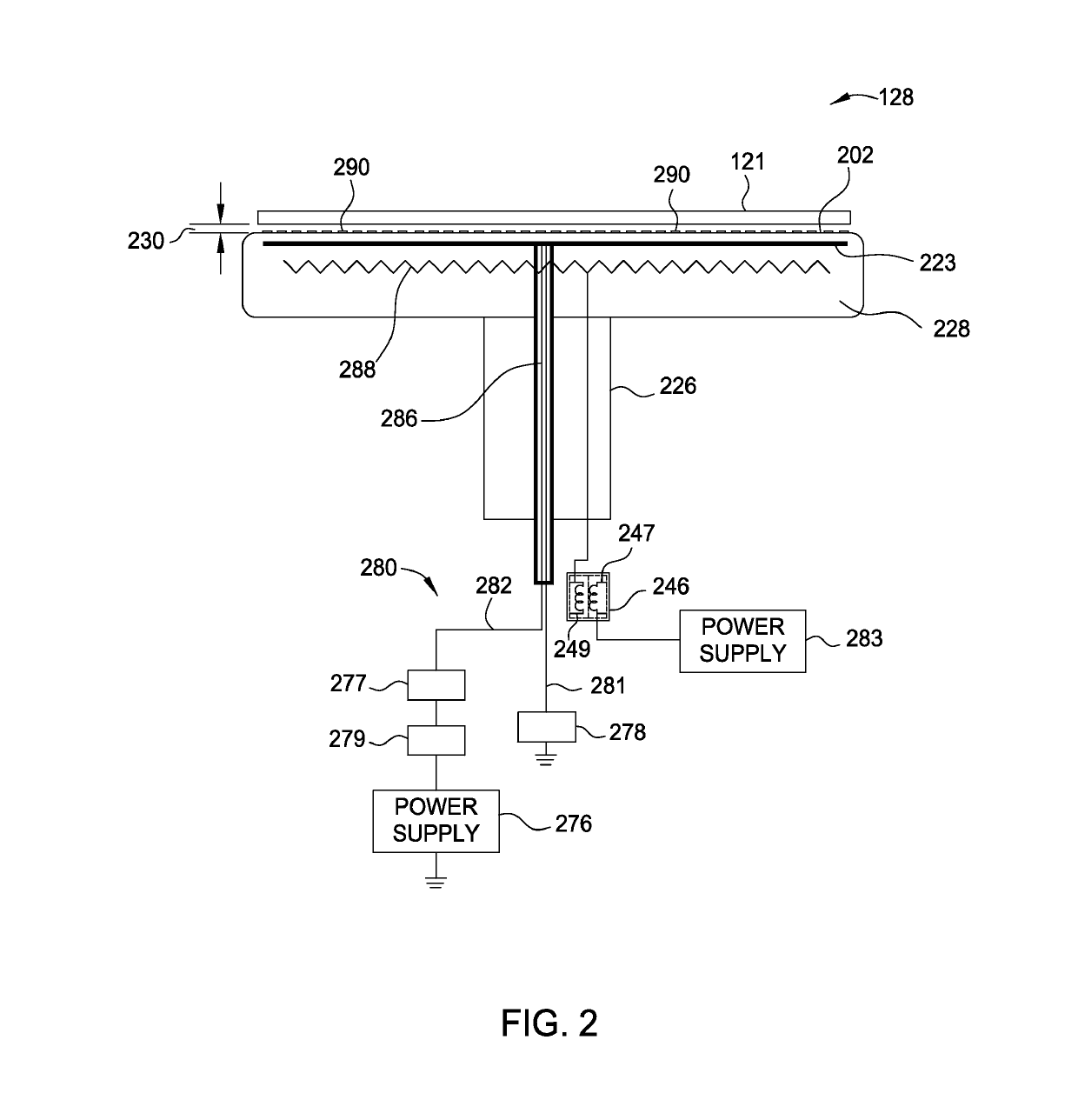
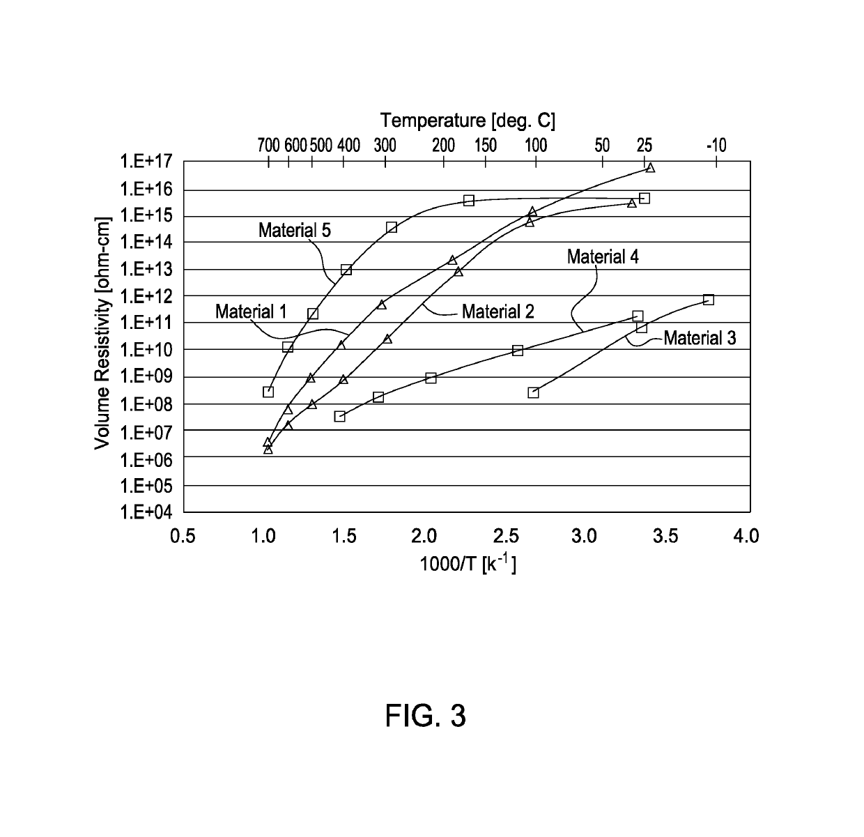
Embodiments of the present disclosure provide an electrostatic chuck for maintaining a flatness of a substrate being processed in a plasma reactor at high temperatures. In one embodiment, the electrostatic chuck comprises a chuck body coupled to a support stem, the chuck body having a substrate supporting surface, and the chuck body has a volume resistivity value of about 1×10⁷ ohm-cm to about 1×10¹⁵ ohm-cm in a temperature of about 250° C. to about 700° C., and an electrode embedded in the body, the electrode is coupled to a power supply. In one example, the chuck body is composed of an aluminum nitride material which has been observed to be able to optimize chucking performance around 600° C. or above during a deposition or etch process, or any other process that employ both high operating temperature and substrate clamping features.
Description
CROSS-REFERENCE TO RELATED APPLICATIONS[0001]This application claims benefit of U.S. provisional patent application Ser. No. 62 / 038,085, filed Aug. 15, 2014, which is herein incorporated by referenceBACKGROUND[0002]Field[0003]Embodiments of the present disclosure generally relate to an apparatus and method for processingsemiconductor substrates. More particularly, embodiments of the present disclosure relate to an electrostatic chuck used in a plasma chamber.[0004]Description of the Related Art[0005]Plasma enhance processes, such as plasma enhanced chemical vapor deposition (PECVD) process, high density plasma chemical vapor deposition (HDPCVD) process, plasma immersion ion implantation process (P3I), and plasma etch process, have become essential in semiconductorprocessing. Plasma provides many advantages in manufacturing semiconductor devices. For example, using plasma enables a wide range of applications due to lowered processing temperature, plasma enhanced deposition has exce...
Claims
Application Information
Patent Timeline
Application Date:The date an application was filed.
Publication Date:The date a patent or application was officially published.
First Publication Date:The earliest publication date of a patent with the same application number.
Issue Date:Publication date of the patent grant document.
PCT Entry Date:The Entry date of PCT National Phase.
Estimated Expiry Date:The statutory expiry date of a patent right according to the Patent Law, and it is the longest term of protection that the patent right can achieve without the termination of the patent right due to other reasons(Term extension factor has been taken into account ).
Invalid Date:Actual expiry date is based on effective date or publication date of legal transaction data of invalid patent.
Patent Type & AuthorityPatents(United States)
IPC IPC(8): H02N13/00H01L21/683H01L21/687
CPCH01L21/6833H01L21/68757H02N13/00H01L21/324
InventorYE, ZHENG JOHNPINSON, II, JAY D.HANAWA, HIROJIZHOU, JIANHUALIN, XINGDUAN, REN-GUANLEE, KWANGDUK DOUGLASKIM, BOK HOENBEHERA, SWAYAMBHU P.HA, SUNGWONBALASUBRAMANIAN, GANESHROCHA-ALVAREZ, JUAN CARLOSKULSHRESHTHA, PRASHANT KUMARFOSTER, JASON K.SRINIVASAN, MUKUNDHALLER, UWE P.PONNEKANTI, HARI K.

