Method for manufacturing compound semiconductor device including p-type impurity layer

a semiconductor device and impurity layer technology, applied in semiconductor devices, semiconductor devices, electrical devices, etc., can solve the problem of difficult sharp change of impurity concentration of p-type base area, and achieve the effect of reducing the absorption of dopan

Active Publication Date: 2019-10-08
DENSO CORP
View PDF11 Cites 0 Cited by
  • Summary
  • Abstract
  • Description
  • Claims
  • Application Information

AI Technical Summary

Benefits of technology

[0009]More specifically, for forming a p-type impurity layer, TMA (the abbreviation of trimethylaluminum) constituting an organic metal material is employed as p-type dopant, for example. In this case, as confirmed by the present inventors, a rise delay that is peculiar to organic metal materials is produced, which prevents a sharp change of the concentration of the p-type impurity layer. The impurity concentration of the p-type base area is therefore difficult to change sharply. Accordingly, the channel length increases, and may cause increase of on-resistance.
[0011]It is an object of the present disclosure to provide a method for manufacturing a compound semiconductor device capable of controlling an impurity concentration profile of a p-type impurity layer with excellent controllability.
[0013]In this case, the pre-doping achieves absorption of the dopant to an inner wall surface of a chamber or other positions beforehand, and reduces absorption of the dopant during epitaxial growth. In addition, the absorption quantity to the chamber is controllable by controlling the time of the pre-doping. In this case, the impurity concentration profile of the p-type impurity layer is controllable. Accordingly, a p-type dopant concentration in an atmosphere inside the chamber, for example, is maintained at a desired concentration from an initial stage of epitaxial growth. In this condition, a sharp change of the impurity concentration of the p-type impurity layer is achievable.

Problems solved by technology

The impurity concentration of the p-type base area is therefore difficult to change sharply.

Method used


Image

  • Method for manufacturing compound semiconductor device including p-type impurity layer
  • Method for manufacturing compound semiconductor device including p-type impurity layer
  • Method for manufacturing compound semiconductor device including p-type impurity layer

Examples


first embodiment

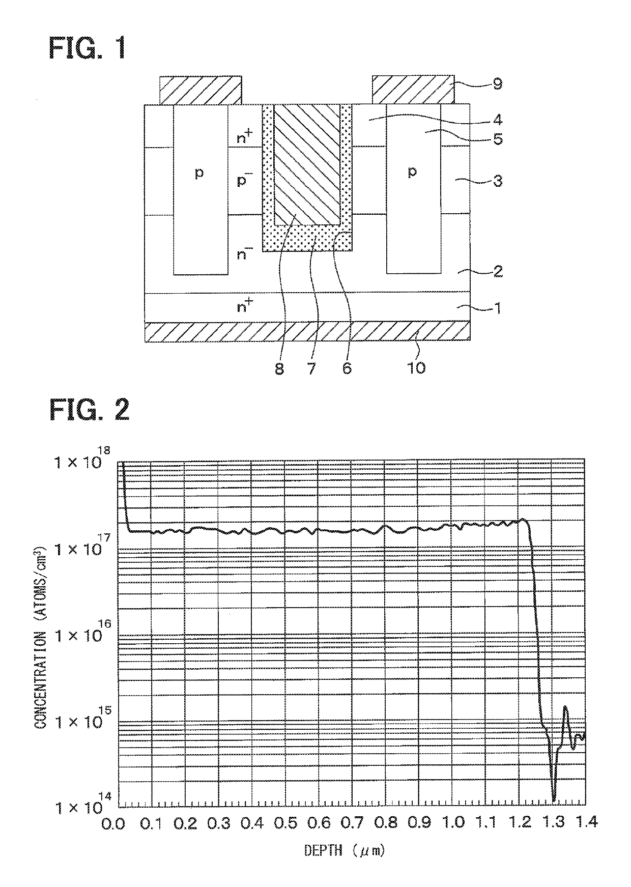
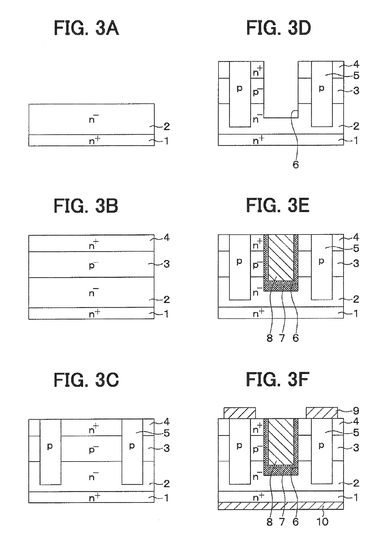
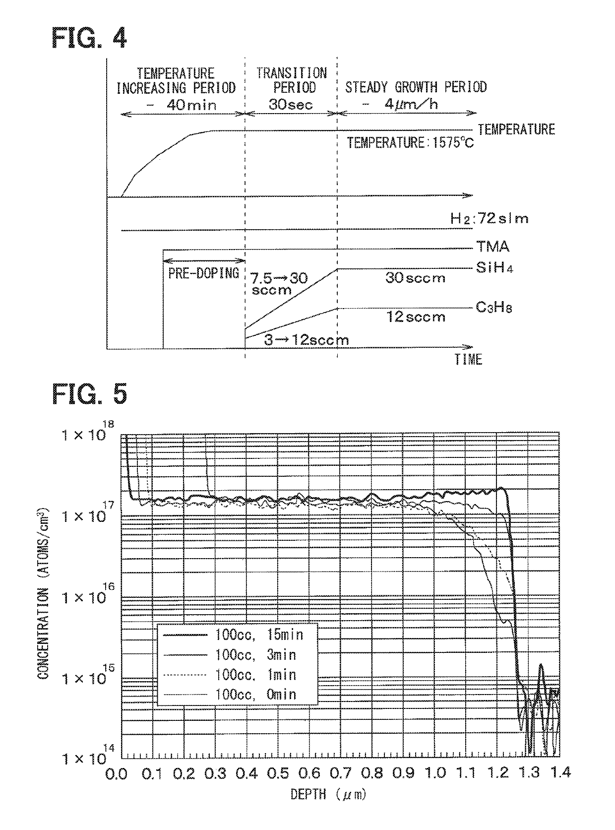
[0024]A first embodiment is now described. A compound semiconductor device described by way of example herein is an SiC semiconductor device that includes a vertical MOSFET having an inverted type trench gate structure.

[0025]An SiC semiconductor device illustrated in FIG. 1 includes a vertical MOSFET having a trench gate structure and disposed in a cell area. The SiC semiconductor device has an outer peripheral resistant structure (not shown) disposed in an outer peripheral area surrounding the cell area.

[0026]The SiC semiconductor device has a semiconductor substrate that includes an n+-type substrate 1 constituting a high-concentration impurity layer composed of SiC, and an n−-type drift layer 2 disposed on a front face side of the n+-type substrate 1 and composed of SiC having an impurity concentration lower than the impurity concentration of the n+-type substrate 1. The n+-type substrate 1 has an n-type impurity concentration of 1.0×10¹⁹ / cm3, for example, while the n−-type drift...

second embodiment

[0059]A second embodiment is now described. The present embodiment is similar to the first embodiment except for the configuration and manufacturing process of the base area 3 that have been changed from the corresponding configuration and process of the first embodiment. Accordingly, only parts different from the corresponding parts of the first embodiment are herein described.

[0060]As illustrated in FIG. 6, the base area 3 according to the present embodiment has a structure constituted by a sequentially lamination of a high-concentration base area 3a that has a relatively high p-type impurity concentration, and a low-concentration base area 3b that has a p-type impurity concentration lower than the p-type impurity concentration of the high-concentration base area 3a.

[0061]For example, the high-concentration base area 3a has a p-type impurity concentration of 5×10¹⁷ / cm3 or higher, such as 1×10¹⁸ / cm3, and has a thickness of 50 nm (nanometers). For example, the low-concentration bas...


PUM


Abstract

A method for manufacturing a compound semiconductor device includes causing epitaxial growth of a p-type impurity layer containing a compound semiconductor on a foundation layer containing the compound semiconductor. The causing the epitaxial growth includes performing pre-doping to preliminarily introduce dopant gas before introducing material gas for the epitaxial growth of the compound semiconductor. The dopant gas contains an organic metal material providing dopant of p-type impurities. An impurity concentration profile of the p-type impurity layer is controlled by controlling a time of the pre-doping.

Description

CROSS REFERENCE TO RELATED APPLICATIONS[0001]This application is a U.S. national phase of International Application No. PCT / JP2017 / 001771 filed on Jan. 19, 2017, and is based on Japanese Patent Application No. 2016-32290 filed on Feb. 23, 2016, the disclosure of which is incorporated herein by reference.TECHNICAL FIELD[0002]The present disclosure relates to a method for manufacturing a compound semiconductor device that includes a compound semiconductor such as silicon carbide (hereinafter referred to as SiC) and gallium nitride (hereinafter referred to as GaN).BACKGROUND ART[0003]Various types of compound semiconductor devices, each including a compound semiconductor such as SiC and GaN, have been proposed. Among these compound semiconductor devices, there is a type provided with a vertical switching element such as a vertical metal-oxide-semiconductor field-effect transistor (MOSFET) that has an inverted type trench gate structure.[0004]The vertical MOSFET having an inverted type ...

Claims


Application Information

Patent Timeline
Patent Type & Authority Patents(United States)
IPC IPC(8): H01G4/38H01L21/02H01L29/16H01L29/78H01L29/66
CPCH01L21/02529H01L29/7813H01L29/66068H01L21/02378H01L21/0262H01L29/1608H01L29/1095H01L29/66734
Inventor TAKEUCHI, YUICHISUZUKI, KATSUMIYAMASHITA, YUSUKE
Owner DENSO CORP
Why Eureka
Try Eureka