Supercharge Your Innovation With Domain-Expert AI Agents!

Silicon-on-insulator structure having bipolar stress, and manufacturing method therefor

a technology of silicon-on-insulator and bipolar stress, which is applied in the direction of semiconductor devices, electrical devices, transistors, etc., can solve the problems of increasing processing speed and power consumption, increasing the difficulty of semiconductor device manufacturing, and advancing toward the physical possible limit, so as to improve the hole mobility of the pmos transistor, improve the hole mobility of the nmos transistor, and improve the electrical characteristics of the transistor

Active Publication Date: 2019-12-03
SHANGHAI HUALI MICROELECTRONICS CORP
View PDF2 Cites 0 Cited by
  • Summary
  • Abstract
  • Description
  • Claims
  • Application Information

AI Technical Summary

Benefits of technology

The present patent provides a method for improving the electrical characteristics of transistors by using a silicon-germanium-on-insulator layer for the PMOS transistor region and a tensile stress silicon-on-insulator layer for the NMOS transistor region. This method has a simple process and strong operability. The technical effect of the patent is to enhance the hole mobility of PMOS and NMOS transistors, thereby improving the overall performance of the transistor.

Problems solved by technology

Over 50 years, the dimension of semiconductors have been significantly reduced, which translates into an increasing processing speed and decreasing power consumption.
Semiconductor device manufacturing has therefore become increasingly challenging and advancing toward the physically possible limit.
However, the electrical characteristics of the semiconductor devices of the current silicon-on-insulator structure still need to be debugged.

Method used


Image

  • Silicon-on-insulator structure having bipolar stress, and manufacturing method therefor
  • Silicon-on-insulator structure having bipolar stress, and manufacturing method therefor
  • Silicon-on-insulator structure having bipolar stress, and manufacturing method therefor

Examples


Embodiment Construction

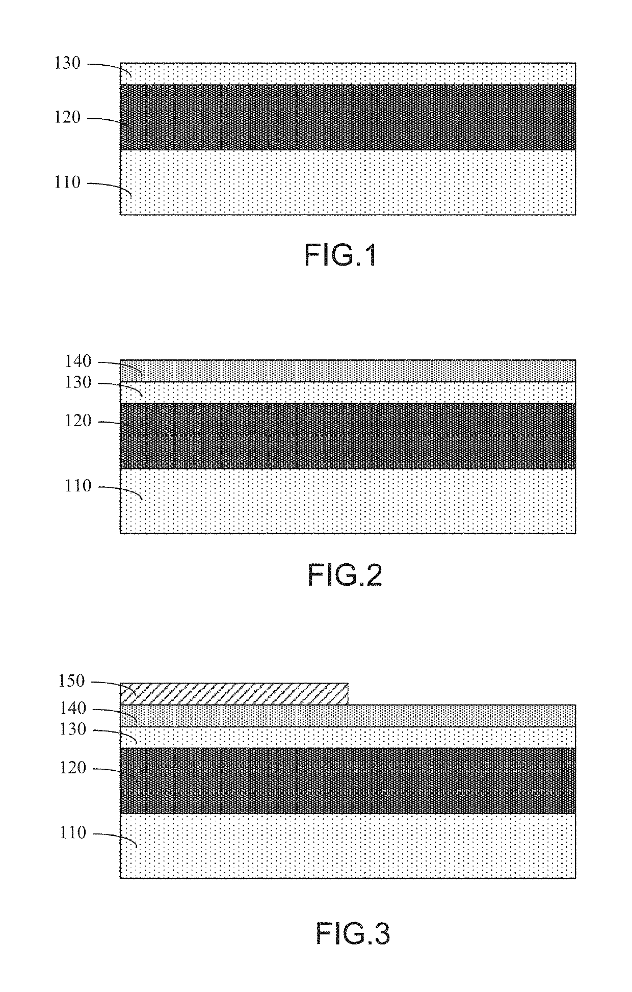
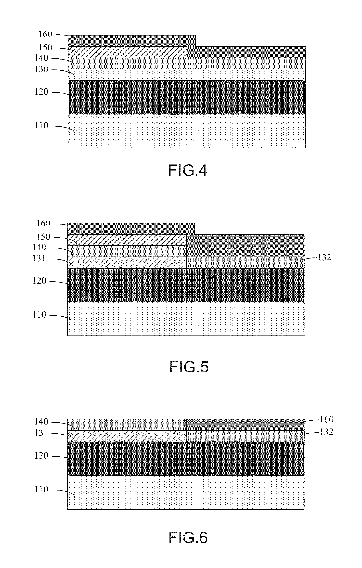
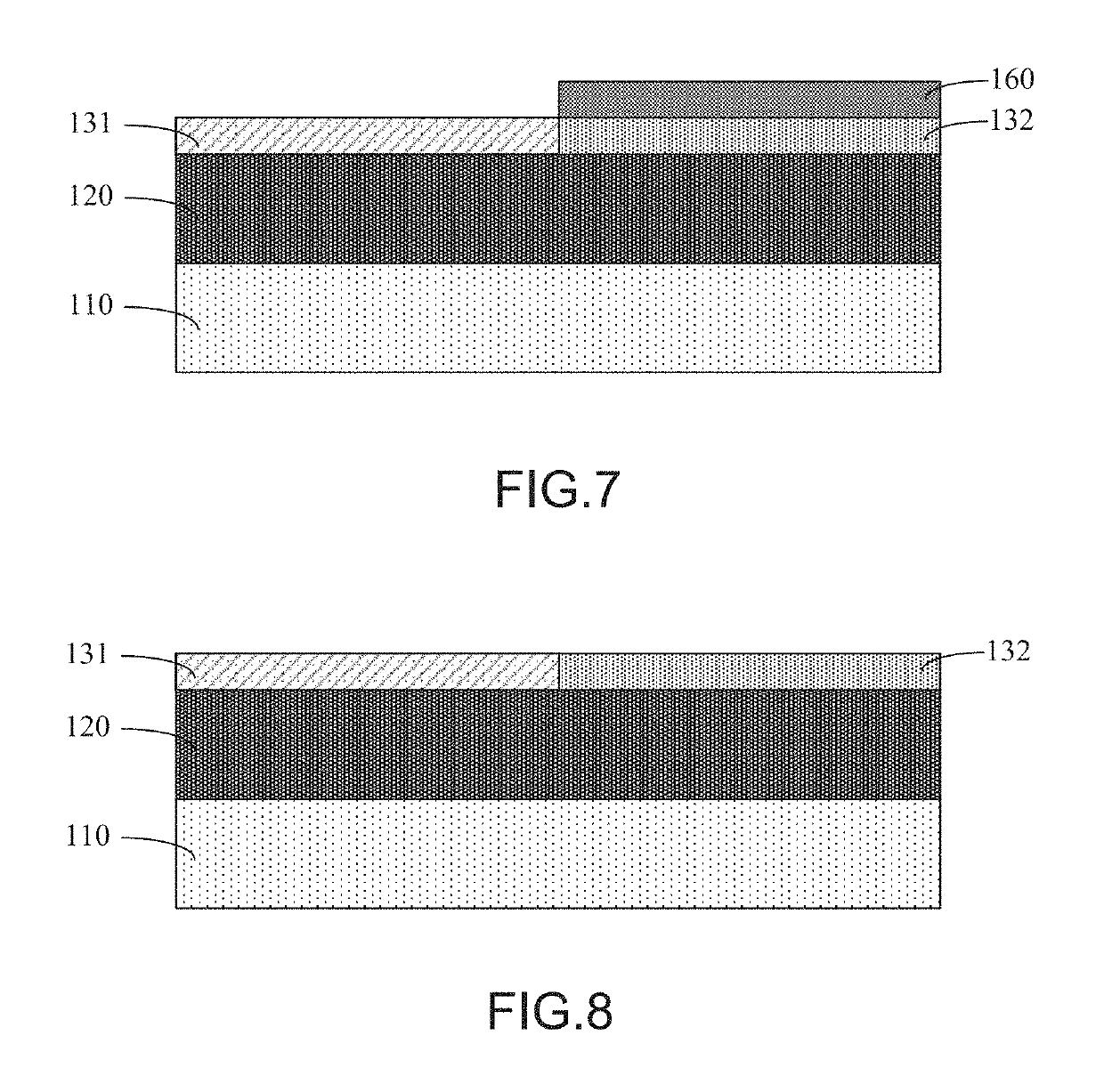
[0020]The present disclosure relates to a semiconductor process and device. The embodiment of the present disclosure provides a silicon-on-insulator structure, wherein the silicon-on-insulator structure has bipolar stress, and a silicon-on-insulator layer corresponding to an NMOS region has a tensile stress, and a silicon-on-insulator structure corresponding to a PMOS region is a silicon-germanium-on-insulator layer, which has compressive stress. The present disclosure also provides other embodiments.

[0021]The reader is cautioned as to all files and documents which are filed at the same time as this specification and which are open for the public to consult, and the contents of all such files and documents are incorporated herein by reference. Unless directly stated otherwise, all features disclosed in this specification (including any appended claims, the abstract, and the accompanying drawings) may be replaced by alternative features serving the same, equivalent, or similar purpos...


PUM

PropertyMeasurementUnit
temperatureaaaaaaaaaa
distanceaaaaaaaaaa
distanceaaaaaaaaaa

Abstract

Provided are a silicon-on-insulator structure having bipolar stress and a manufacturing method therefor. The manufacturing method comprises providing a composite substrate, wherein the composite substrate has a silicon substrate layer, a buried oxide layer and a silicon-on-insulator layer sequentially from bottom to top, epitaxially growing a silicon germanium layer on an upper surface of the silicon-on-insulator layer; depositing a hard mask layer to cover a portion of the silicon germanium layer corresponding to an N-type MOS transistor region; depositing a surface oxide layer to cover the silicon germanium layer and the hard mask layer; performing a high temperature annealing treatment so that a portion of the silicon-on-insulator layer corresponding to a P-type MOS transistor region is converted into a silicon-germanium-on-insulator layer, and the portion corresponding to the N-type MOS transistor region is converted into a tensile stress silicon-on-insulator layer.

Description

CROSS-REFERENCES TO RELATED APPLICATIONS[0001]The present application claims priority to Chinese Patent Application No. 201810286263.1, filed on Mar. 30, 2018, entitled “SILICON-ON-INSULATOR STRUCTURE HAVING BIPOLAR STRESS, AND MANUFACTURING METHOD THEREFOR”, which is incorporated by reference herein for all purposes.TECHNICAL FIELD[0002]The present disclosure relates to semiconductor elements, and particularly to a silicon-on-insulator structure containing bipolar stress and a manufacturing method therefor.BACKGROUND OF THE INVENTION[0003]Since the invention of integrated circuits by Dr. Jack Kilby of Texas Instruments in early years, scientists and engineers have made numerous inventions and improvements in semiconductor devices and processes. Over 50 years, the dimension of semiconductors have been significantly reduced, which translates into an increasing processing speed and decreasing power consumption. To date, the development of semiconductors has largely followed Moore's La...

Claims


Application Information

Patent Timeline
Patent Type & Authority Patents(United States)
IPC IPC(8): H01L27/12H01L21/02H01L21/28H01L21/762H01L29/161H01L29/72
CPCH01L29/72H01L21/02532H01L21/76229H01L27/1203H01L21/28176H01L29/161H01L21/84H01L27/092H01L29/7842H01L21/823807H01L21/76264
Inventor MA, YANFEIWANG, CHANGFENGLIAO, DUANQUAN
Owner SHANGHAI HUALI MICROELECTRONICS CORP
Features
  • R&D
  • Intellectual Property
  • Life Sciences
  • Materials
  • Tech Scout
  • Unparalleled Data Quality
  • Higher Quality Content
  • 60% Fewer Hallucinations
Learn More