Semiconductor package structure

a semiconductor and package technology, applied in semiconductor lasers, printed circuit aspects, printed circuit non-printed electric components association, etc., can solve the problems of reducing the angle of limiting the capability of semiconductor package structure in signal transmission and receiving, and reducing the overall thickness of an electronic produ

Active Publication Date: 2020-02-11
EVERLIGHT ELECTRONICS
View PDF5 Cites 0 Cited by
  • Summary
  • Abstract
  • Description
  • Claims
  • Application Information

AI Technical Summary

Benefits of technology

[0009]An objective of the present invention is to provide a semiconductor package structure which is not entirely disposed on the surface of a printed circuit board (PCB), so the semiconductor package structure protrudes less on the surface of the printed circuit board (PCB), thereby reducing the overall thickness of an electronic product.
[0010]An objective of the present invention is to provide another semiconductor package structure, which can improve or prevent the shift of the solder on the printed circuit board (PCB) so that a plurality of semiconductor package structures can be arranged on the printed circuit board (PCB) more densely.
[0011]An objective of the present invention is to provide another semiconductor package structure, which comprises a first substrate and a second substrate to advantageously form particular structures such as protrusions or solder receiving portions or the like to achieve the effect of protruding less on the printed circuit board (PCB) or improving the shift of the solder.

Problems solved by technology

However, the reduction in the volume is not only limited by the manufacturing capability, but also is limited by design requirements of the semiconductor package structure.
However, in this way, the angle for signal transmitting and receiving is reduced, thereby limiting the capability of the semiconductor package structure in signal transmitting and receiving.
However, when the side view light emitting device is soldered onto a printed circuit board (PCB), the solder on a soldering region of the printed circuit board (PCB) may be shifted by being pressed, thereby causing problems such as short circuit caused by contact of the solder with other devices, conductors or electrodes or the like.
In order to prevent these problems, a certain distance needs to be maintained between the side view light emitting devices, and this makes denser arrangement impossible.
Additionally, the light emitting device often comprises encapsulant which may be silicone, and the silicone intends to collapse and deform when being baked at a high temperature so that the silicone cannot maintain a predetermined shape (i.e., an encapsulant collapsing phenomenon will occur).
If the conventional methyl-based silicone of high thixotropy is used as the encapsulant, the hardness of the encapsulant after being cured is insufficient although the encapsulant is less likely to collapse.
Moreover, the humidity resistance or the sulfur resistance of the methyl-based silicone is also relatively poor.
Accordingly, there are still many problems to be solved in the technical field of the semiconductor package structure.

Method used


Image

  • Semiconductor package structure
  • Semiconductor package structure
  • Semiconductor package structure

Examples


Embodiment Construction

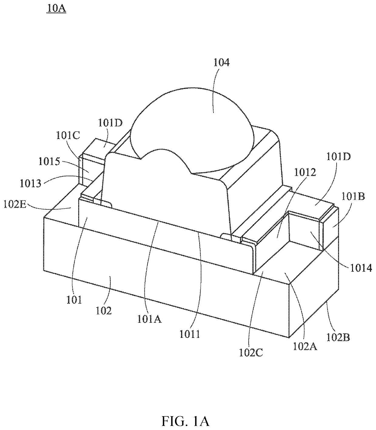
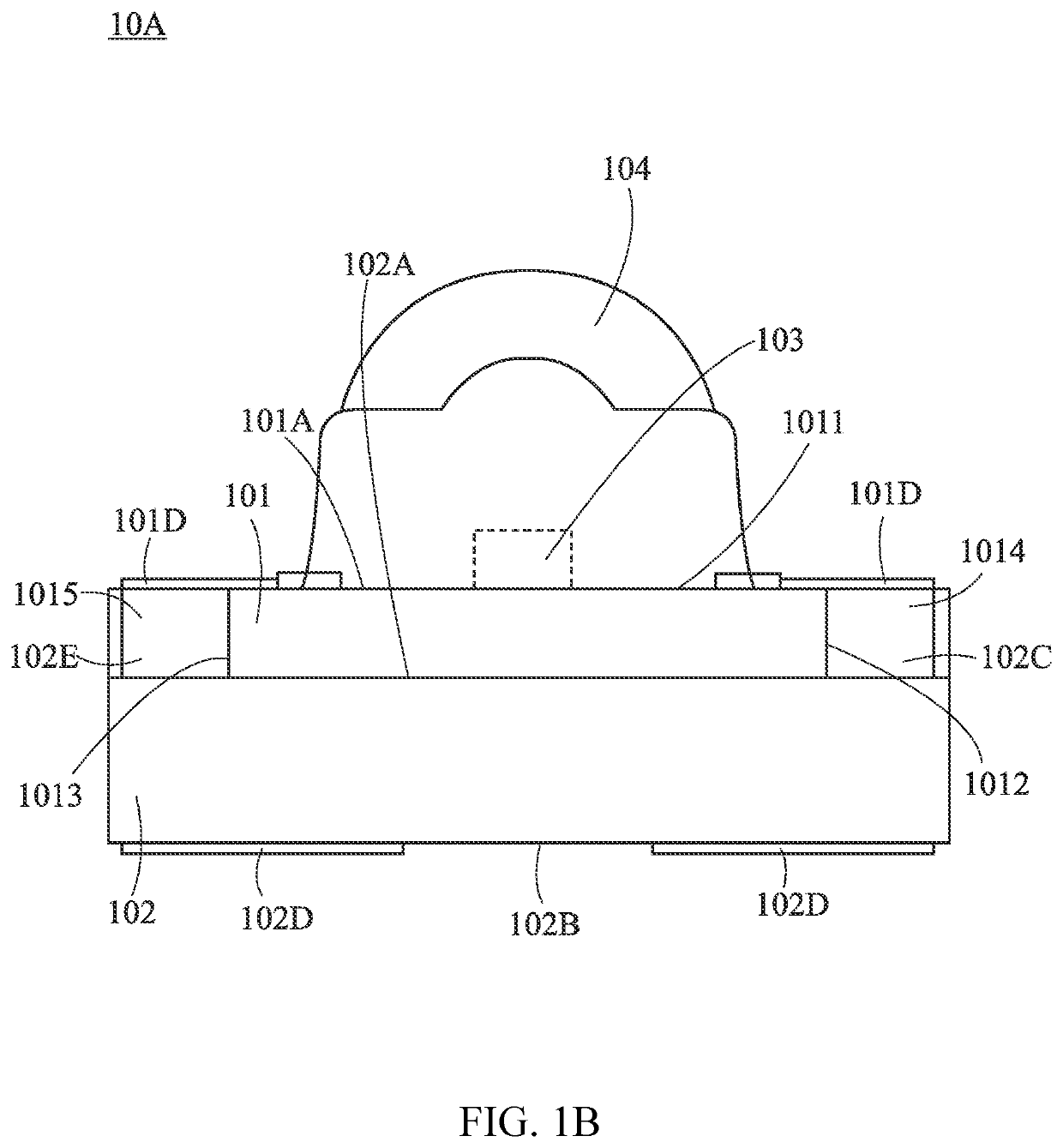
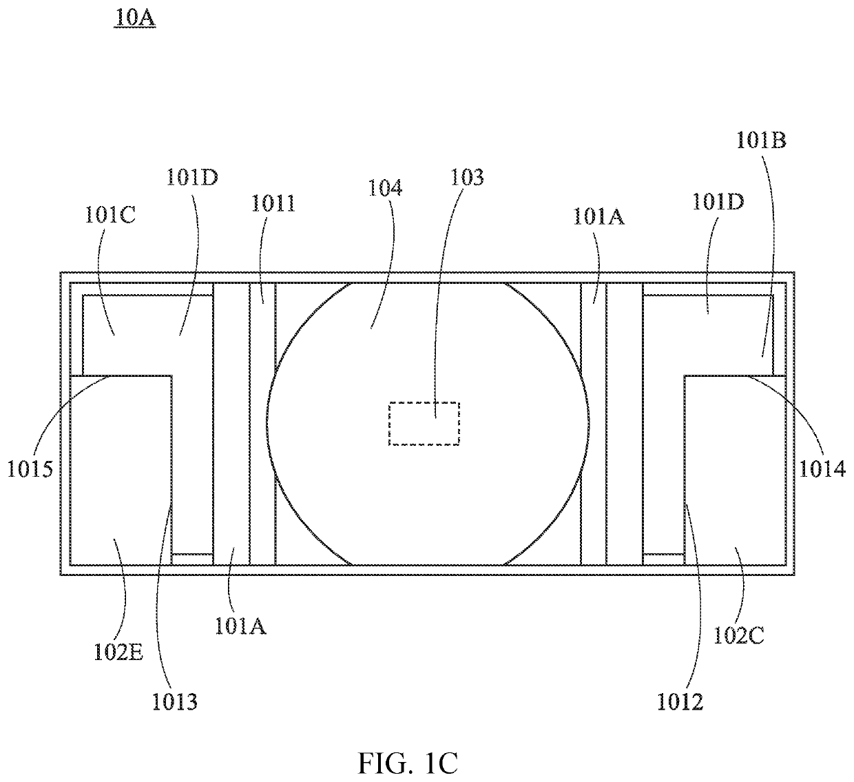
[0143]A part of specific embodiments of the present invention will be described specifically hereinafter. However, the present invention may be implemented by embodiments of various forms without departing from the spirit of the present invention, and the claimed scope of the present invention should not be construed as being limited to what described in the specification. Additionally, technical contents of various implementations in the above summary may also serve as technical contents of the embodiments or as possible variants of the embodiments. Moreover, orientations described above (e.g., front, back, upper, lower, two sides or the like) are relative orientations and may be defined according to use states (e.g., the side view type) of the semiconductor package structure.

[0144]Referring to FIG. 1A to FIG. 1D, which are a schematic perspective view and corresponding schematic plane views of a semiconductor package structure 10A (which is called a package structure 10A hereinaft...


PUM

PropertyMeasurementUnit
refractive indexaaaaaaaaaa
light emitting wavelengthaaaaaaaaaa
particle diameteraaaaaaaaaa

Abstract

A semiconductor package structure is disclosed. The package structure includes a first substrate, a second substrate on which the first substrate is disposed, and a semiconductor chip which is disposed on the first substrate. The two substrates can include two notches or two solder receiving portions. Therefore, when the package structure is disposed on the printed circuit board (PCB), the package structure will protrude less on the surface of the printed circuit board (PCB); or, the solders on the printed circuit board (PCB) will not be shifted by the package structure.

Description

CROSS-REFERENCES TO RELATED APPLICATIONS[0001]This application claims priorities to a U.S. Provisional Application No. 62 / 550,694 filed on Aug. 27, 2017, a U.S. Provisional Application No. 62 / 613,056 filed on Jan. 3, 2018 and a U.S. Provisional Application No. 62 / 651,609 filed on Apr. 2, 2018, all of which are incorporated by reference herein in their entirety.BACKGROUND OF THE INVENTIONField of the Invention[0002]The present invention relates to a package structure, and more particularly, relates to a semiconductor package structure.Descriptions of the Related Art[0003]A semiconductor chip (e.g., an IC chip, an LED chip and a sensor chip or the like) is commonly disposed in a package structure so that the package structure may protect the semiconductor chip to a certain degree; and an assembly of the semiconductor chip and the package structure may be referred to as a semiconductor package structure.[0004]The semiconductor package structure has been applied to various electronic pr...

Claims


Application Information

Patent Timeline
Patent Type & Authority Patents(United States)
IPC IPC(8): H01L33/54H01L23/00H01S5/022H01L23/31H01L23/13H01L33/48H05K1/18H01L31/02H01L31/0203H01L33/56H01L33/62H05K3/34H05K1/11H01S5/02315H01S5/0233
CPCH01L33/54H01S5/02236H01L31/0203H01L33/486H01L33/56H01L33/62H05K1/184H01L31/02005H01L2924/00012H01L2924/12041H01L2224/45099H05K2201/09063H01L2924/181H01L2224/48227H01L2924/00014H01L2924/12043H01L2224/48464H01L2224/48091H05K1/111H05K3/34H01L24/48H01L23/13H01L23/3121H01S5/0233H01S5/02315H01L25/0657H01L23/3135H01L24/14H01L24/16H01S5/0235
Inventor HO, CHIH-MINGLIANG, CHUN-CHIHCHERNG, DING-HWALU, KUANG-MAOLO, WEN-CHUEHYANG, HAO-YUKANG, CHIEH-YUPAN, HAN-CHANG
Owner EVERLIGHT ELECTRONICS
Why Eureka
Try Eureka